SEMICONDUCTOR DEVICE INCLUDING h-BN INSULATING LAYER AND ITS MANUFACTURING METHOD

a technology of insulating layer and semiconductor, which is applied in the direction semiconductor devices, electrical devices, etc., can solve the problems of insufficient heat dissipation effect of insulating layer, inability to completely dissipate heat from the semiconductor body through the substrate body, and the deterioration of semiconductor light-emitting devices, etc., to achieve efficient dissipation and large thermal conductivity

Active Publication Date: 2016-06-09
STANLEY ELECTRIC CO LTD
View PDF4 Cites 7 Cited by
  • Summary
  • Abstract
  • Description
  • Claims
  • Application Information

AI Technical Summary

Benefits of technology

[0011]According to the presently disclosed subject matter, since the h-BN particles have an extremely large thermal conductivity, heat generated from the semiconductor element is efficiently dissipated via the insulating layer including the h-BN particles to the support substrate.

Problems solved by technology

In the above-described prior art semiconductor light-emitting device, however, since the thermal conductivity of the insulating layer made of silicon dioxide is low, the heat dissipating effect of the insulating layer is insufficient, so that it is impossible to completely dissipate heat from the semiconductor body through the substrate body.
Thus, due to the generation of heat by the semiconductor body, the semiconductor light-emitting device would deteriorate and its lifetime would he shortened.

Method used


Image

  • SEMICONDUCTOR DEVICE INCLUDING h-BN INSULATING LAYER AND ITS MANUFACTURING METHOD
  • SEMICONDUCTOR DEVICE INCLUDING h-BN INSULATING LAYER AND ITS MANUFACTURING METHOD
  • SEMICONDUCTOR DEVICE INCLUDING h-BN INSULATING LAYER AND ITS MANUFACTURING METHOD

Examples


first embodiment

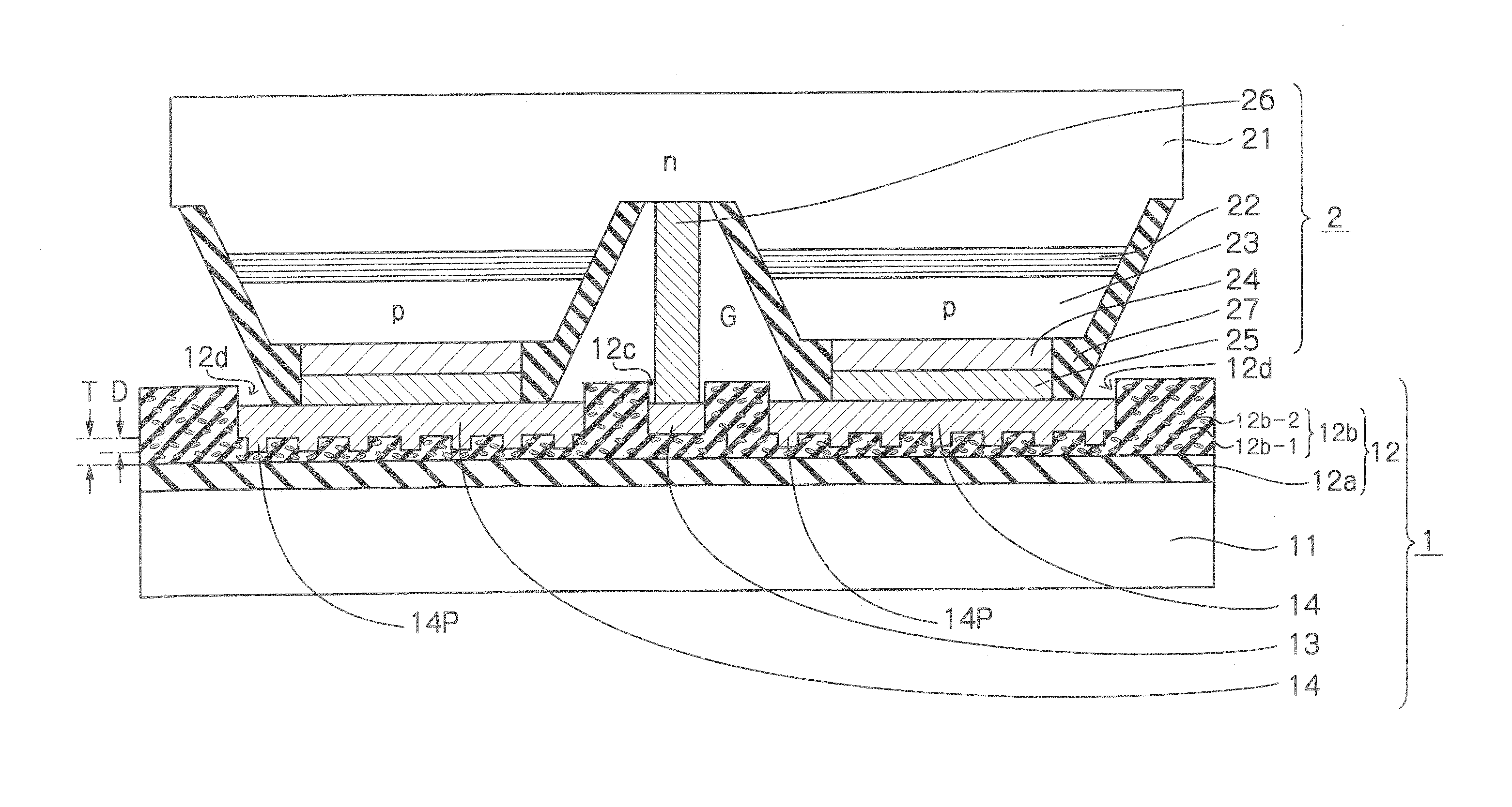
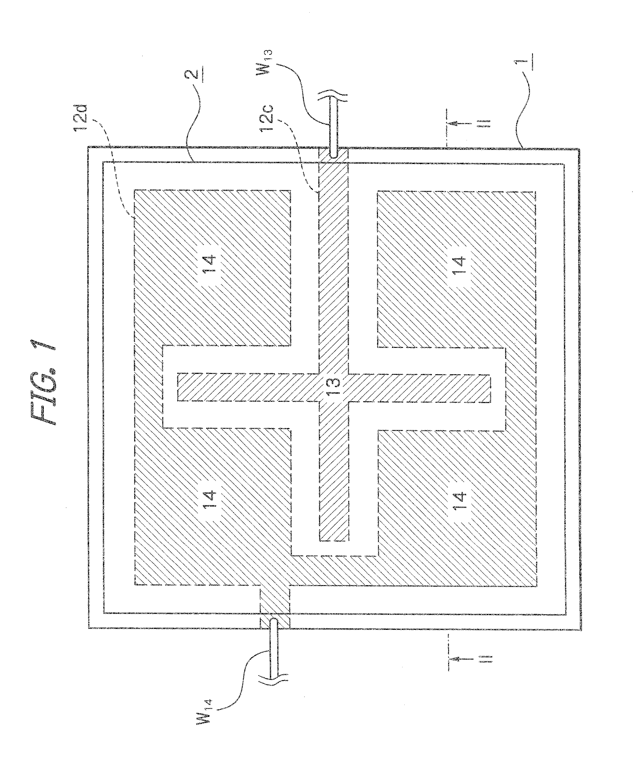
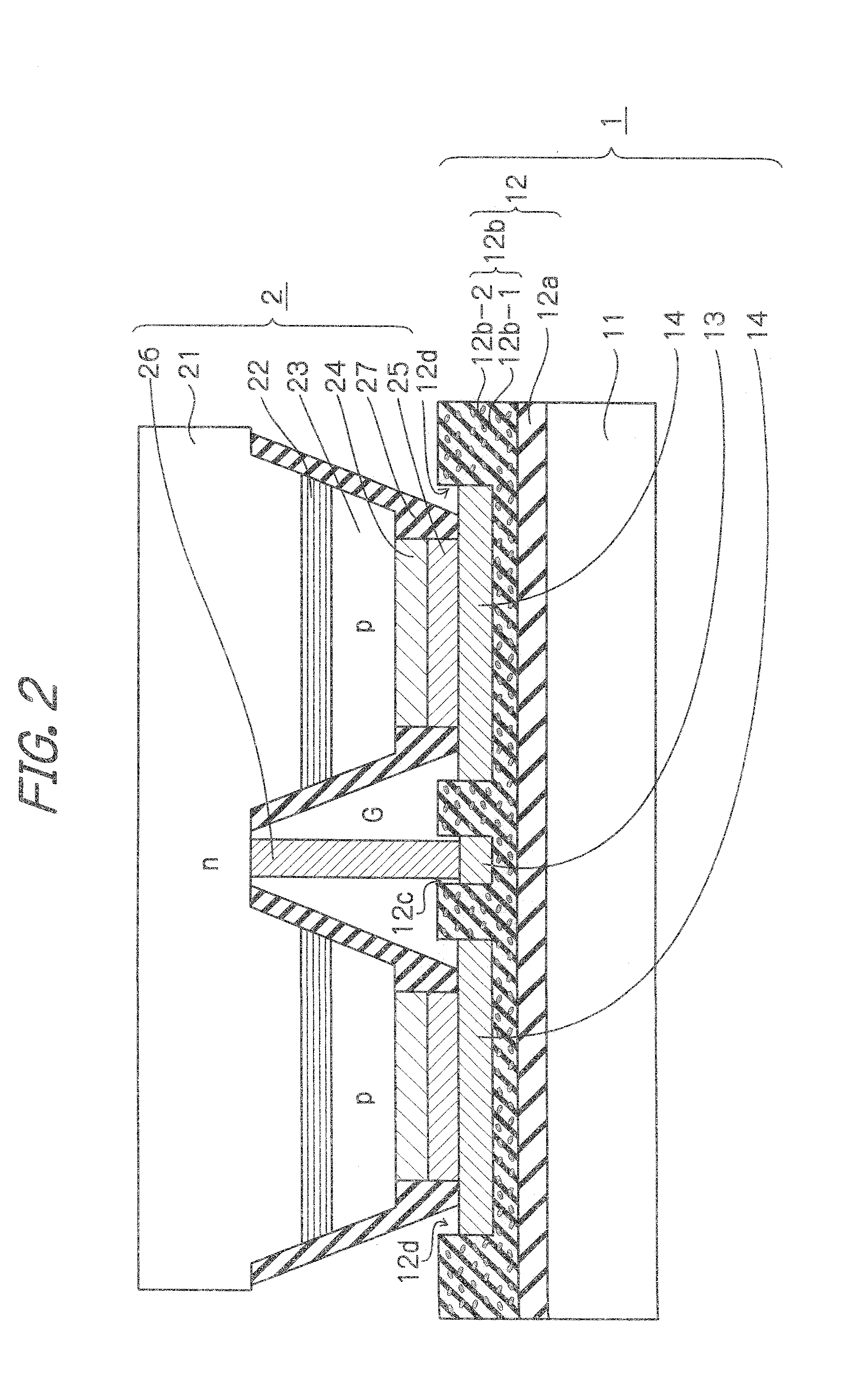
[0032]FIG. 1 illustrates the semiconductor light-emitting device according to the presently disclosed subject matter, and FIG. 2 is a cross-sectional view taken along the line II-II in FIG. 1,

[0033]In FIGS. 1 and 2, the semiconductor light-emitting device is constructed by a support body 1 and a semiconductor body 2 supported by the support body 1.

[0034]The support body includes a support substrate 11 made of heat dissipating material such as Si, an insulating layer 12 formed on the support substrate 11, an n-side wiring layer 13 and a p-side wiring layer 14.

[0035]In more detail, the insulating layer 12 is constructed by a lower insulating (buffer) layer 12a made of amorphous boron nitride (a-BN) formed directly on the support substrate 11 and an upper insulating (heat dissipating) layer 12b made of amorphous boron nitride (a-BN) 12b-1 containing hexagonal system boron nitride (h-BN) particles 12b-2 whose a-axes have an large extremely large thermal conductivity λa-axis larger than ...

second embodiment

[0071]FIG. 8 illustrates the semiconductor light-emitting device according to the presently disclosed subject matter, and FIG. 9 is a cross-sectional view taken along the line IX-IX in FIG. 8.

[0072]In FIGS. 8 and 9, a grid-shaped groove GG is formed at the recess 12d in the upper insulating layer 12b, so that the p-side wiring layer 14 has protrusions 14P penetrated into the upper insulating layer 12b. As a result, the vertical transfer of heat from the bonding layer 25 via the upper insulating layer 12b to the support substrate 11 is enhanced while the horizontal transfer of heat within the upper insulating layer 12b is mitigated. Thus, the heat dissipating effect can be further enhanced as compared with the first embodiment.

[0073]The grid-shaped groove GG in the upper insulating layer 12b at the recess 12d can be formed by performing a dry etching process upon the upper insulating layer 12b using a photomask before the formation of the wiring layers 13 and 14.

[0074]FIG. 10 is a pl...


PUM

PropertyMeasurementUnit
thermal conductivityaaaaaaaaaa
temperatureaaaaaaaaaa
pressureaaaaaaaaaa

Abstract

A semiconductor device includes a support substrate, an insulating layer provided on the support substrate, and a semiconductor element provided on the insulating layer. The insulating layer has a lower insulating layer consisting of amorphous boron nitride, and an upper insulating layer provided on the lower insulating layer and including amorphous boron nitride and an hexagonal system boron nitride (h-BN) particles.

Description

[0001]This application claims the priority benefit under 35 U.S.C. §119 to Japanese Patent Application No. JP2014-245825 filed on Dec. 4, 2014, which disclosure is hereby incorporated in its entirety by reference.BACKGROUND[0002]1. Field[0003]The presently disclosed subject matter relates to a semiconductor device and its manufacturing method.[0004]2. Description of the Related Art[0005]Generally, a semiconductor light-emitting device formed by a light-emitting diode (LED) element is used as a backlight for a liquid crystal, display (LCD) apparatus, a light for an industrial apparatus and the like.[0006]A prior art semiconductor light-emitting device is constructed by thermally-pressuring a semiconductor body to a support body which includes a support substrate made of heat dissipating material such as silicon (Si), an insulating layer formed on the support substrate made of silicon dioxide, and wiring layers formed on the insulating layer (see: JP2014-120511A).[0007]In the above-de...

Claims


Application Information

Patent Timeline
Patent Type & Authority Applications(United States)
IPC IPC(8): H01L21/02H01L33/20H01L33/44H01L21/3105
CPCH01L21/02172H01L21/02266H01L33/44H01L33/20H01L21/3105H01L33/08H01L33/62H01L21/02112
Inventor TANAKA, KAZUFUMI
Owner STANLEY ELECTRIC CO LTD
Why Eureka
Try Eureka