Semiconductor device and fabricating method thereof

a semiconductor device and semiconductor technology, applied in the field of semiconductor devices, can solve the problems of inability to meet the device performance demand, and the performance of the semiconductor devices containing the above-described existing fin fet remains problemati

Active Publication Date: 2017-02-02
SEMICONDUCTOR MANUFACTURING INTERNATIONAL (BEIJING) CORP +1
View PDF3 Cites 5 Cited by
  • Summary
  • Abstract
  • Description
  • Claims
  • Application Information

AI Technical Summary

Benefits of technology

[0036]On the other hand, comparing to the thermal conductivity of the traditional material of silicon oxide, the thermal conductivity of aluminum nitride is much higher, which is up to 150 W / mK-180 W / mK. Additionally, aluminum nitride has desired properties including high pressure-resistance, high temperature-resistance, and high corrosion-resistance. By using the aluminum nitride as the material of the insulating layer for isolating the fins, the heat dissipation of the semiconductor device can be improved, and the insulation performance of semiconductor devices in a complex environment can also be effectively improved as well.
[0036]On the other hand, comparing to the thermal conductivity of the traditional material of silicon oxide, the thermal conductivity of aluminum nitride is much higher, which is up to 150 W / mK-180 W / mK. Additionally, aluminum nitride has desired properties including high pressure-resistance, high temperature-resistance, and high corrosion-resistance. By using the aluminum nitride as the material of the insulating layer for isolating the fins, the heat dissipation of the semiconductor device can be improved, and the insulation performance of semiconductor devices in a complex environment can also be effectively improved as well.
[0012]In some embodiments, the semiconductor device further comprises an oxide layer formed on the side walls of the plurality of fins, wherein the insulating layer covers the oxide layer.
[0014]Another aspect of the disclosed subject matter provides a method for forming a semiconductor device, comprising: providing a semiconductor substrate including a plurality of fins projected on a surface of the semiconductor substrate; forming an insulating film on top portions and side walls of the plurality of fins, wherein the insulating film is located on the surface of the semiconductor substrate, and a thermal conductivity of the insulating layer is larger than a thermal conductivity of silicon oxide; and etching a portion of the insulating film to expose top surfaces and a part of side walls of the plurality of fins and to form an insulating layer that has a surface lower than the top surfaces of the plurality of fins.

Problems solved by technology

However, when the critical dimension (CD) of the device further decreases, even with the gate-last process, the conventional MOS field effect transistor structure is unable to meet the demand of the device performance.
However, with further size decreasing of the process node, the performance of the semiconductor devices that contain the above-described existing fin FET remains problematic.

Method used


Image

  • Semiconductor device and fabricating method thereof
  • Semiconductor device and fabricating method thereof
  • Semiconductor device and fabricating method thereof

Examples


Embodiment Construction

[0032]Various objects, features, and advantages of the disclosed subject matter can be more fully appreciated with reference to the following detailed description of the disclosed subject matter when considered in connection with the following drawings, in which like reference numerals identify like elements. It should be noted that the following drawings are merely examples for illustrative purposes according to various disclosed embodiments and are not intended to limit the scope of one disclosure.

[0033]It is apparent that the described embodiments are some but not all of the embodiments of the present invention. Based on the disclosed embodiments, persons of ordinary skill in the art may derive other embodiments consistent with the present disclosure, all of which are within the scope of the present invention.

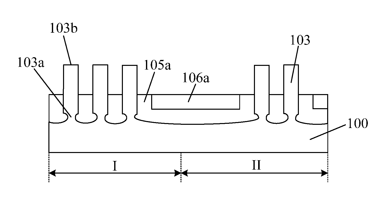
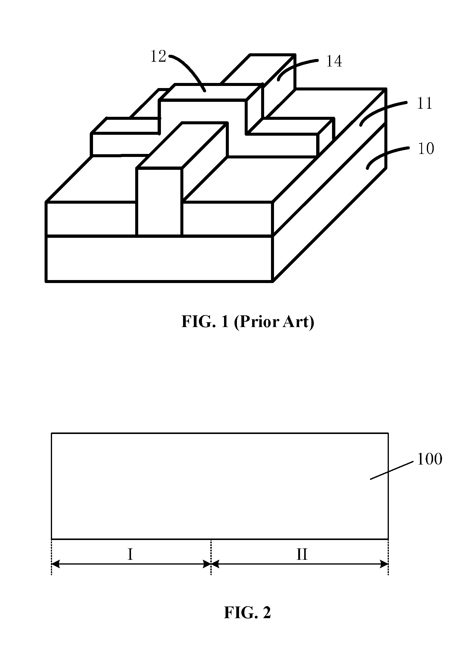
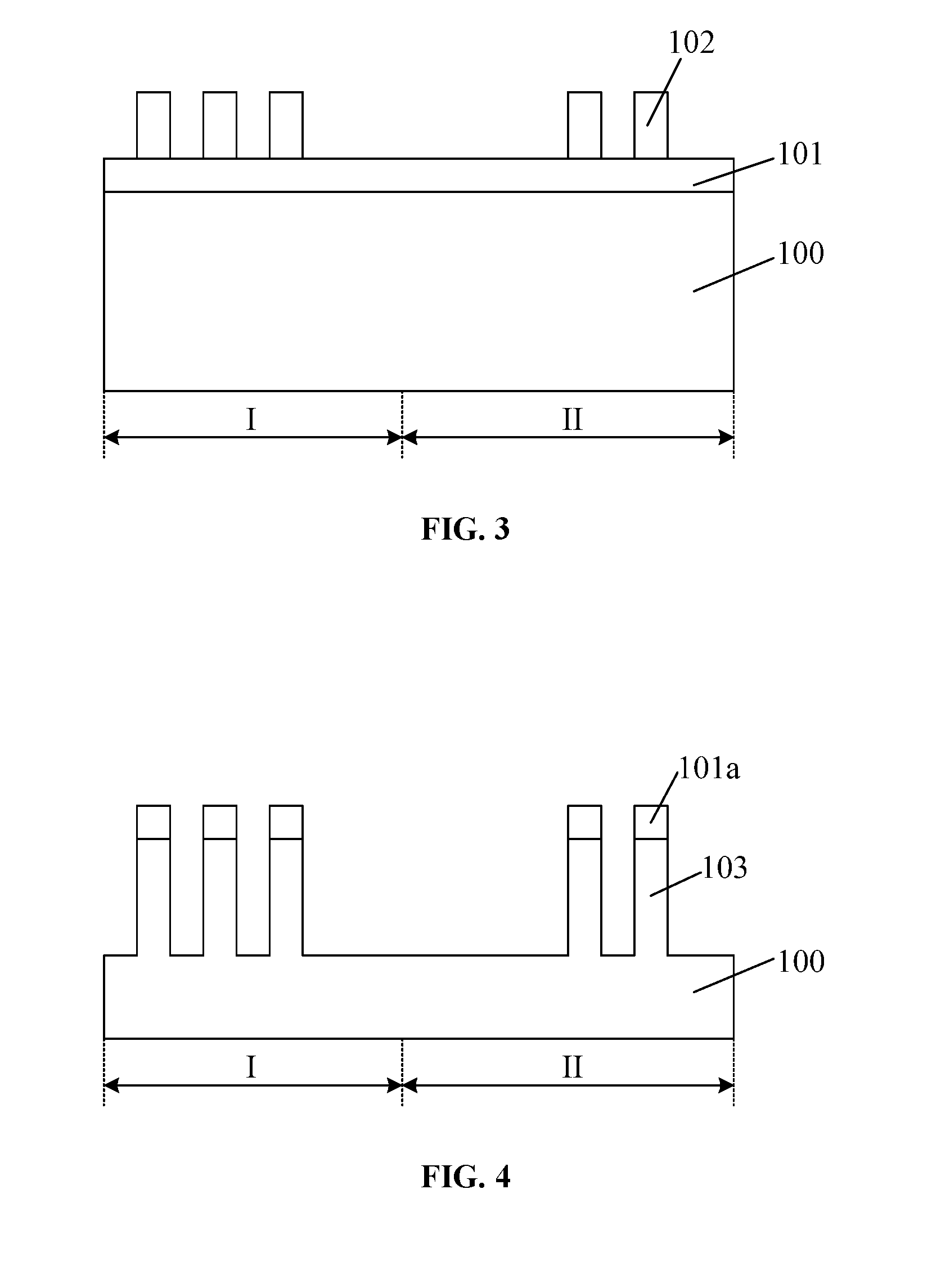
[0034]As mentioned in the background section, the performance of the semiconductor devices that contain the existing fin FET remains problematic.

[0035]For example, a silicon...


PUM


Abstract

In accordance with various embodiments of the disclosed subject matter, a semiconductor device, and a fabricating method thereof are provided. In some embodiments, the semiconductor device comprises: a semiconductor substrate, wherein a plurality of fins are projected on a surface of the semiconductor substrate; and an insulating layer on side walls of the plurality of fins, wherein the insulating layer is located on the surface of the semiconductor substrate, a surface of the insulating layer is lower than top surfaces of the plurality of fins, and a thermal conductivity of the insulating layer is larger than a thermal conductivity of silicon oxide.

Description

CROSS-REFERENCES TO RELATED APPLICATIONS[0001]This application claims the priority of Chinese patent application No. 201510456885.0, filed on Jul. 29, 2015, the entire content of which is incorporated herein by reference.TECHNICAL FIELD[0002]The disclosed subject matter generally relates to semiconductor technology and, more particularly, relates to a semiconductor device, and a fabricating method thereof.BACKGROUND[0003]With the continuous development of semiconductor technology and the continuous decreasing of the process node, gate-last technology has been widely used to obtain a desired threshold voltage and an improved device performance. However, when the critical dimension (CD) of the device further decreases, even with the gate-last process, the conventional MOS field effect transistor structure is unable to meet the demand of the device performance. Therefore, multi-gate devices, as an alternative to the conventional devices, have been widely considered.[0004]A fin field ef...

Claims


Application Information

Patent Timeline
Patent Type & Authority Applications(United States)
IPC IPC(8): H01L29/40H01L29/78H01L21/3105H01L21/02H01L21/762H01L29/06H01L29/66
CPCH01L29/408H01L29/0653H01L29/7851H01L21/31053H01L21/0228H01L21/02178H01L21/76232H01L29/66795H01L21/823431H01L27/0211H01L27/0886H01L23/3677H01L21/76229H01L21/30608H01L21/3065H01L21/3083H01L21/76224
Inventor XIE, XINYUNZHOU, MING
Owner SEMICONDUCTOR MANUFACTURING INTERNATIONAL (BEIJING) CORP
Why Eureka
Try Eureka