Array Substrate and Manufacturing Method Thereof and Liquid Crystal Display Panel Using the Array Substrate

a technology which is applied in the field of array substrate and manufacturing method thereof, can solve the problems of direct affecting the displaying quality of images, images on the screen may show phenomena and achieve the effects of enhancing uniformity of voltage, reducing parasitic capacitance, and improving the phenomenon of greenish and flickering of images on the screen

Active Publication Date: 2016-07-07
SHENZHEN CHINA STAR OPTOELECTRONICS TECH CO LTD
View PDF4 Cites 13 Cited by
  • Summary
  • Abstract
  • Description
  • Claims
  • Application Information

AI Technical Summary

Benefits of technology

[0008]An object of the present invention is to provide an array substrate, which takes advantage of a black matrix formed thereon to reduce a parasitic capacitance between a common electr

Problems solved by technology

Thus, the uniformity of the voltage on the common electrode directly affect the displaying quality of images.
When the vol

Method used


Image

  • Array Substrate and Manufacturing Method Thereof and Liquid Crystal Display Panel Using the Array Substrate
  • Array Substrate and Manufacturing Method Thereof and Liquid Crystal Display Panel Using the Array Substrate
  • Array Substrate and Manufacturing Method Thereof and Liquid Crystal Display Panel Using the Array Substrate

Examples


Embodiment Construction

[0046]To further expound the technical solution adopted in the present invention and the advantages thereof, a detailed description is given to a preferred embodiment of the present invention and the attached drawings.

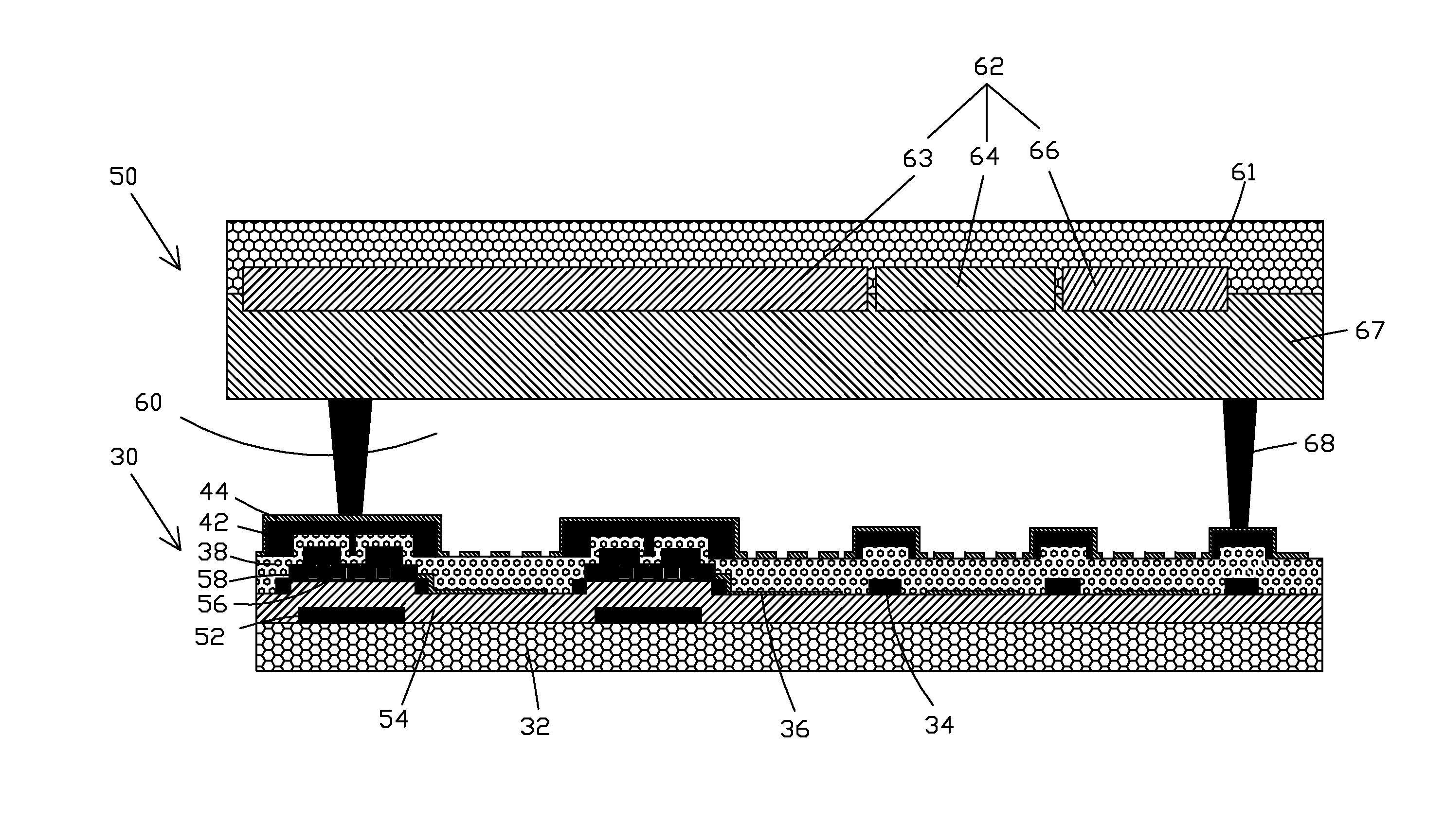
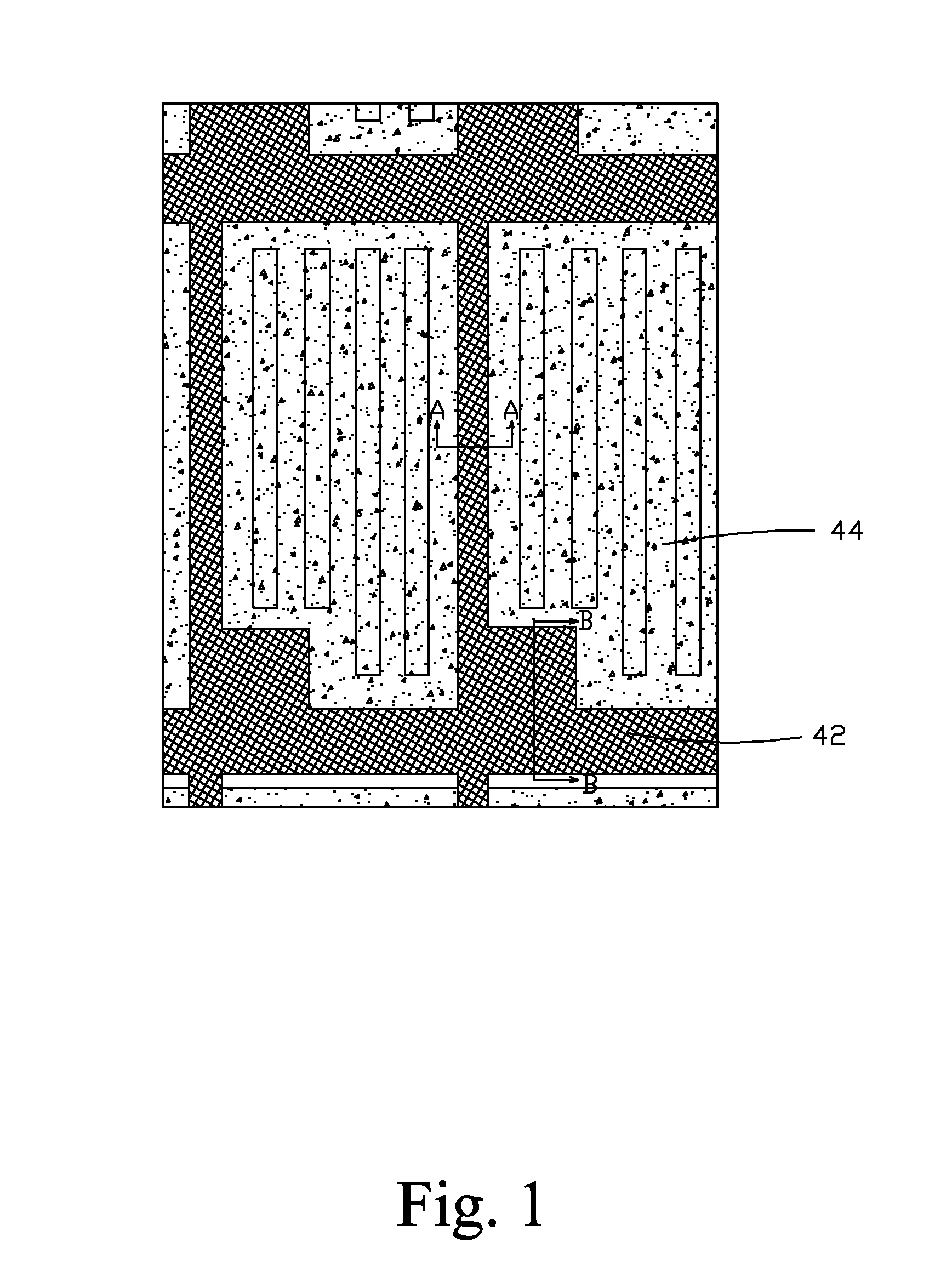
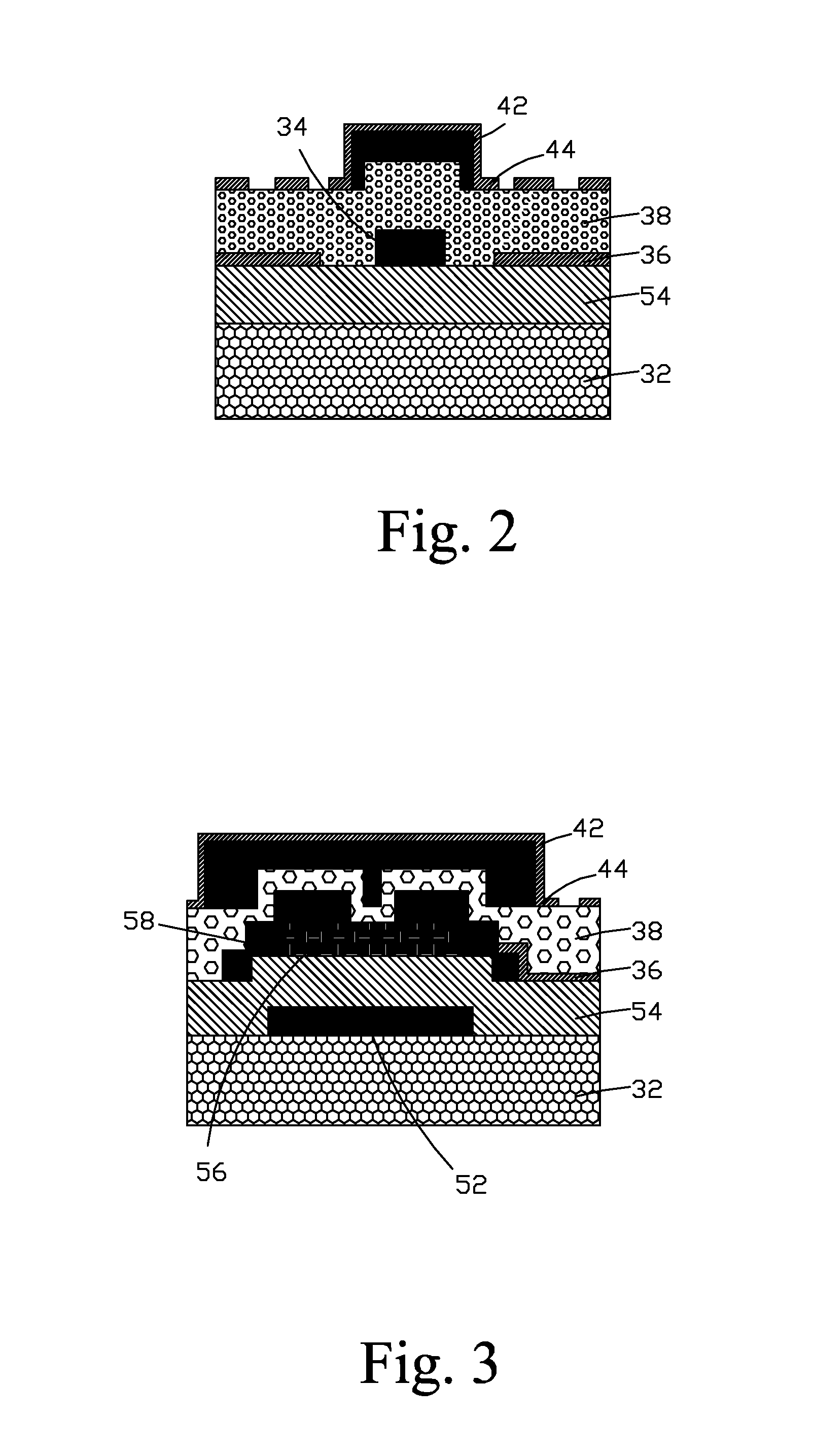
[0047]Referring to FIGS. 1-3, the present invention provides an array substrate. The array substrate is applicable to an FFS (Fringe Field Switching) display panel and comprises, specifically: a first substrate 32, a gate line (not shown) formed on the first substrate 32, a data line 34 formed on the first substrate 32, a thin-film transistor array (not labeled) formed on the first substrate 32, a pixel electrode 36 formed on the thin-film transistor array, a first passivation layer 38 formed on the pixel electrode 36, the data line 34, and the thin-film transistor array, a black matrix 42 formed on the first passivation layer 38, and a common electrode 44 formed on the black matrix 42 and the first passivation layer 38. The common electrode 44 is located above the dat...


PUM


Abstract

The present invention provides an array substrate and a manufacturing method thereof and a liquid crystal display panel using the array substrate. The array substrate includes: a first substrate (32), a gate line formed on the first substrate (32), a data line (34) formed on the first substrate (32), a thin-film transistor array formed on the first substrate (32), a pixel electrode (36) formed on the thin-film transistor array, a first passivation layer (38) formed on the pixel electrode (36), the data line (34), and the thin-film transistor array, a black matrix (42) formed on the first passivation layer (38), and a common electrode (44) formed on the black matrix (42) and the first passivation layer (38). The present invention arranges the black matrix formed on the array substrate to reduce the parasitic capacitance between the common electrode and the gate line and the data line so as to help enhance uniformity of voltage on the common electrode.

Description

BACKGROUND OF THE INVENTION[0001]1. Field of the Invention[0002]The present invention relates to the field of liquid crystal display technology, and in particular to an array substrate and a manufacturing method thereof and a display panel using the array substrate.[0003]2. The Related Arts[0004]Liquid crystal displays (LCDs) have a variety of advantages, such as thin device body, low power consumption, and being free of radiation, and are thus widely used. The development of the liquid crystal display industry brings in severer and severer performance requirements, such as performance related to high resolution, high brightness, wide view angle, and low power consumption, and associated techniques have been developed. Most of the liquid crystal displays that are currently available in the market are backlighting liquid crystal displays, which comprise a liquid crystal display panel and a backlight module. The operation principle of the liquid crystal display panel is that, with liq...

Claims


Application Information

Patent Timeline
IPC IPC(8): G02F1/1368H01L29/49H01L29/786H01L29/423G02F1/1339H01L21/027H01L29/66G02F1/1362G02F1/1335H01L27/12H01L21/02
CPCG02F1/1368G02F2001/136295H01L29/4908H01L29/495H01L27/1222H01L27/1218H01L29/78669H01L29/42364H01L29/42372H01L27/1259H01L21/02274H01L21/02532H01L21/02592H01L21/0262H01L21/0274H01L29/66765G02F1/136286G02F1/133512G02F1/133514G02F1/1339H01L27/124H01L29/78633G02F1/136209G02F1/134372G02F1/13606G02F1/133302G02F1/136295G02F1/133345G02F1/13439G02F2201/121G02F2201/123G02F2202/103H01L27/1262H01L27/127
Inventor XU, XIANGYANG
Owner SHENZHEN CHINA STAR OPTOELECTRONICS TECH CO LTD
Why Eureka
Try Eureka