This helps you quickly interpret patents by identifying the three key elements:
Problems solved by technology
Method used
Benefits of technology
Benefits of technology
The present disclosure is a semiconductor device that reduces electric resistance and enhances mechanical strength while being easily mounted face-down.
Problems solved by technology
The semiconductor device including the above semiconductor element is difficult to miniaturize after the device has been packaged.
Method used
Image
Click on the blue label to locate the original text in one second.
Reading with bidirectional positioning of images and text.
Examples
first exemplary embodiment
Variation 2 of First Exemplary Embodiment
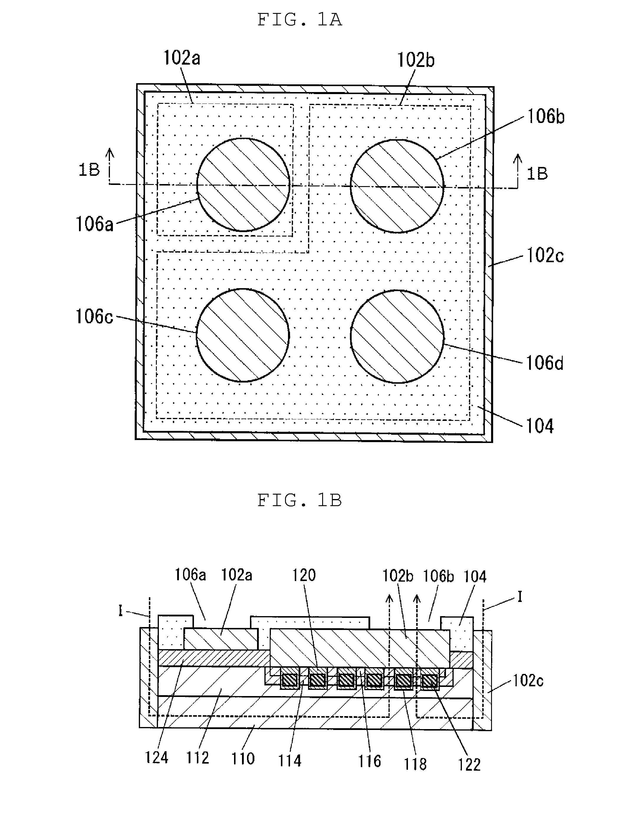
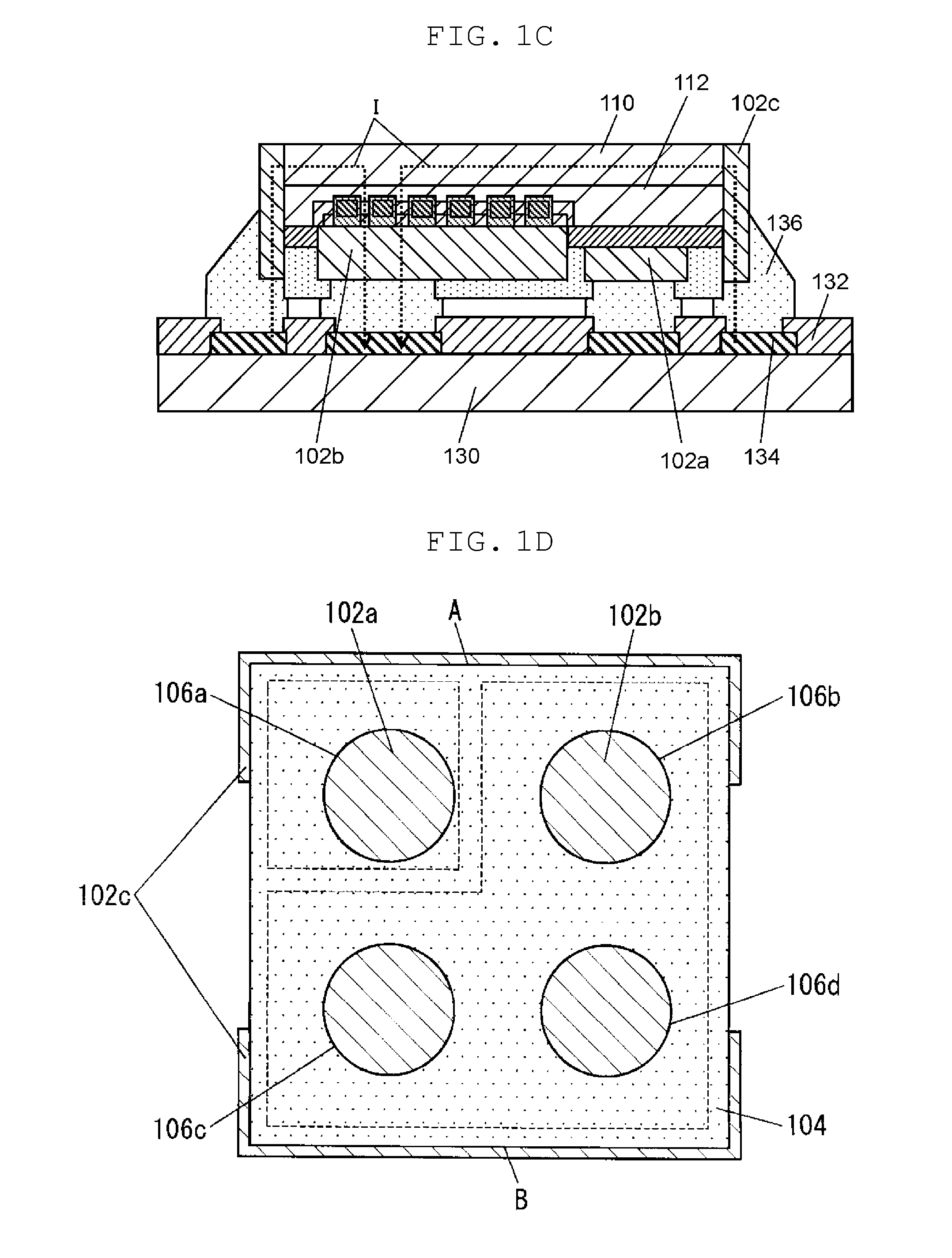
[0083]Hereinafter, a semiconductor device in variation 2 of the first exemplary embodiment will be described with reference to FIG. 1E.
[0084]The semiconductor device in variation 2 differs from the semiconductor device shown inn FIGS. 1A and 1B in a configuration that contact region 126 having lower resistance than semiconductor layer 110 is formed between semiconductor layer 110 and conductor film 102c.
[0085]In this variation, in a case where a conductivity type of semiconductor layer 110 is the N type, an impurity concentration of contact region 126 is preferably 1×10²⁰ [cm3] or more. In a case where the conductivity type of semiconductor layer 110 is the P type, the concentration of contact region 126 is preferably 1×10¹⁹ [ / cm3] or more.
[0086]In a case where conductor film 102c is made of Mo, Cr, Ti, W, Ni, Au, Pt, Al, or Co by an electron beam (EB) vapor deposition method which is included in a physical vapor deposition (PVD) method, con...
second exemplary embodiment
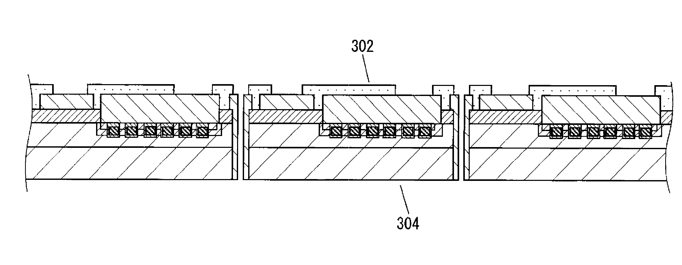
[0110]Hereinafter, a semiconductor device in the second exemplary embodiment in the present disclosure will be described with reference to FIGS. 4A to 4D.
[0111]FIG. 4A is a plan view of the semiconductor device in the second exemplary embodiment. A broken line shows conductor films 402a and 402b under protective film 404.
[0112]As shown in FIG. 4A, the semiconductor device includes conductor film 402a, conductor film 402b surrounded by conductor film 402a, and protective film 404 formed on the conductor films. Two openings 406a and 406b are provided in protective film 404 for conductor film 402a, while one opening 406c is provided in protective film 404 for conductor film 402b. Each of conductor film 402a, conductor film 402b, and conductor film 402c provided on each of opposite side surfaces of the semiconductor device serves as an external terminal.
[0113]FIG. 4B is a plan view of the semiconductor device mounted on mounting substrate 130. FIG. 4B is a through-view of a portion othe...
third exemplary embodiment
[0120]Hereinafter, a semiconductor device in the third exemplary embodiment in the present disclosure will be described with reference to FIGS. 5A and 5B. FIG. 5A is a plan view of the semiconductor device. FIG. 5B is a cross-sectional view of the semiconductor device taken along line 5B-5B in FIG. 5A.
[0121]Protective film 500 is formed on a side surface of the semiconductor device, that is, on conductor film 102c. Protective film 500 preferably has an insulating property. Protective film 500 is made of, for example, siliconoxide, siliconnitride, organic material, resin, silicone, metaloxide, or composed of composite material of the above materials, or may have laminated layers of the above materials. Protective film 500 may be formed by a CVD method.
[0122]In a manufacturing process of the semiconductor device including a mounting process, in order to reduce manufacturing costs by shortening a manufacturing time per semiconductor device, manufacturing speed is increased to maximu...
PUM
Abstract
A semiconductor device includes a semiconductor layer, a first conductor film, a second conductor film, and a first protective film. The semiconductor layer has a semiconductor element. The first conductor film is formed on an upper surface of the semiconductor layer and is electrically. connected to the semiconductor element. The second conductor film is formed on an outer side surface of the semiconductor layer and is electrically connected to the semiconductor element. The first protective film is formed on the first conductor film and has an opening to expose the first conductor film. A height from the upper surface of the semiconductor layer to an upper surface of the second conductor film is equal to or smaller than a height from the upper surface of the semiconductor layer to an upper surface of the first conductor film.
Description
RELATED APPLICATIONS[0001]This application is a Continuation of International Application No. PCT / JP2014 / 004927, filed on Sep. 26, 2014, which in turn claims priority from Japanese Patent Application No. 2013-206071, filed on Oct. 1, 2013, the contents of all of which are incorporated herein by reference in their entireties.BACKGROUND[0002]1. Field of the Invention[0003]The present disclosure relates to a semiconductor device.[0004]2. Description of the Related Art[0005]The semiconductor device is provided by singulating and packaging a semiconductor wafer, on which semiconductor elements are formed through processes such as diffusing and wiring, to be connected to an external circuit. A great number of such semiconductor devices are mounted in an electronic device.[0006]In the semiconductor device, a structure in which a major current path is formed between an upper surface and a lower surface of the semiconductor element is used in the semiconductor element such as a metaloxide s...
Claims
Application Information
Patent Timeline
Application Date:The date an application was filed.
Publication Date:The date a patent or application was officially published.
First Publication Date:The earliest publication date of a patent with the same application number.
Issue Date:Publication date of the patent grant document.
PCT Entry Date:The Entry date of PCT National Phase.
Estimated Expiry Date:The statutory expiry date of a patent right according to the Patent Law, and it is the longest term of protection that the patent right can achieve without the termination of the patent right due to other reasons(Term extension factor has been taken into account ).
Invalid Date:Actual expiry date is based on effective date or publication date of legal transaction data of invalid patent.

