Semiconductor device

US20160218058A1Active Publication Date: 2016-07-28NEXPERIA BV

Image

  • Semiconductor device
  • Semiconductor device
  • Semiconductor device

Examples


first embodiment

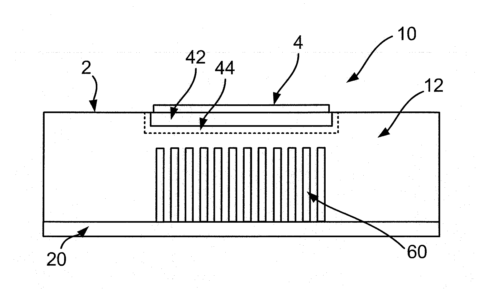
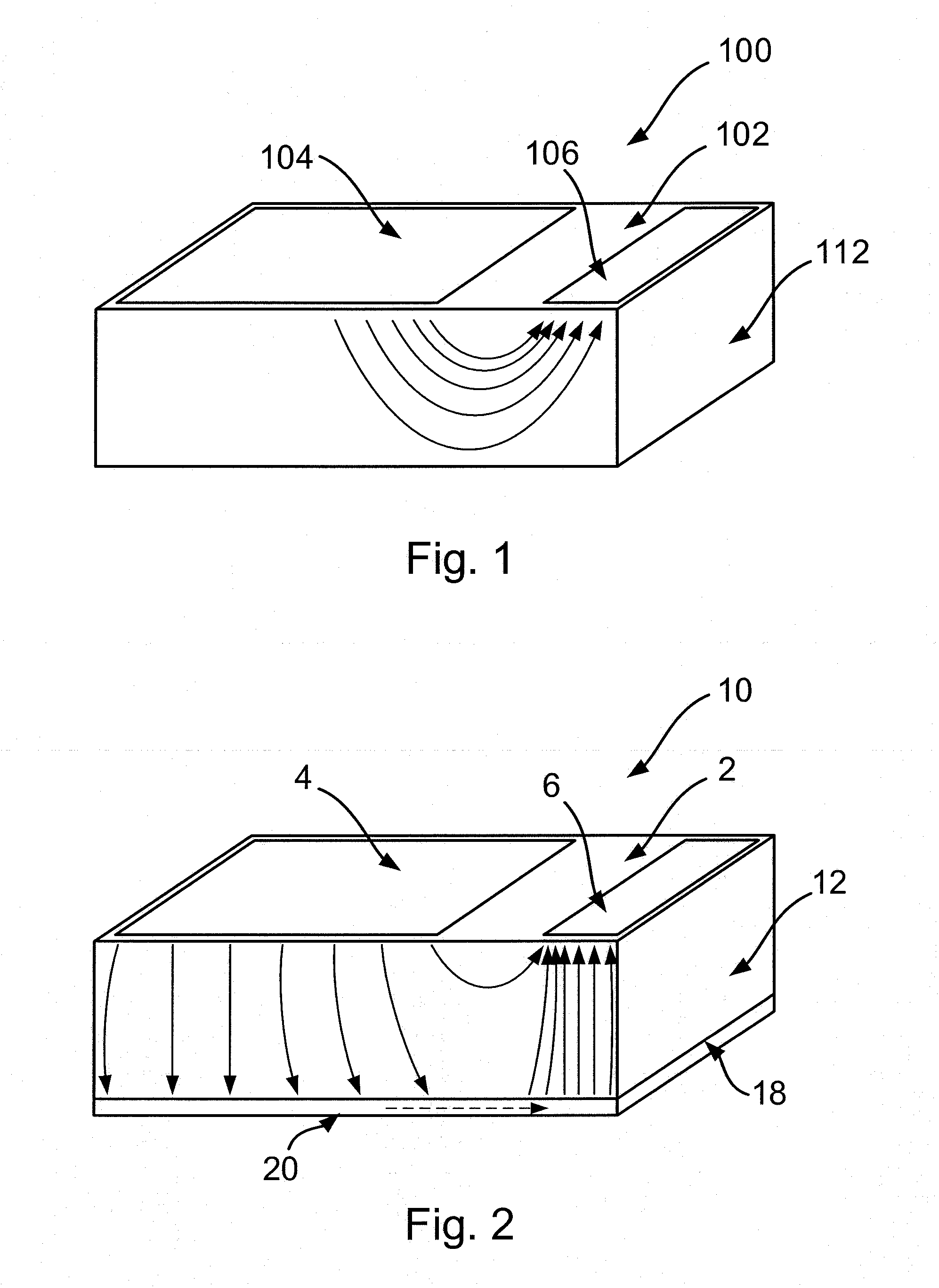
[0036]FIG. 2 shows a semiconductor device 10 according to this invention. The semiconductor device 10 includes a semiconductor substrate 12. The substrate 12 may, for example, comprise silicon or any other suitable semiconductor material. As will be described later in more detail, the substrate 12 may be a die that is diced from a larger wafer during manufacture.

[0037]In accordance with embodiments of this invention, the substrate 12 is provided in a chip-scale package (CSP). Accordingly, the substrate 12 includes a plurality of contacts that are provided on a major surface 2 thereof. In this example, the plurality of contacts includes a first contact 4 and a second contact 6. This embodiment may, for instance, include a pn-junction diode or a Schottky diode in which the first contact 4 is a cathode of the diode and the second contact 6 is an anode of the diode. As described above, the substrate 12 can be mounted on a carrier such as a printed circuit board (PCB), with the first con...

second embodiment

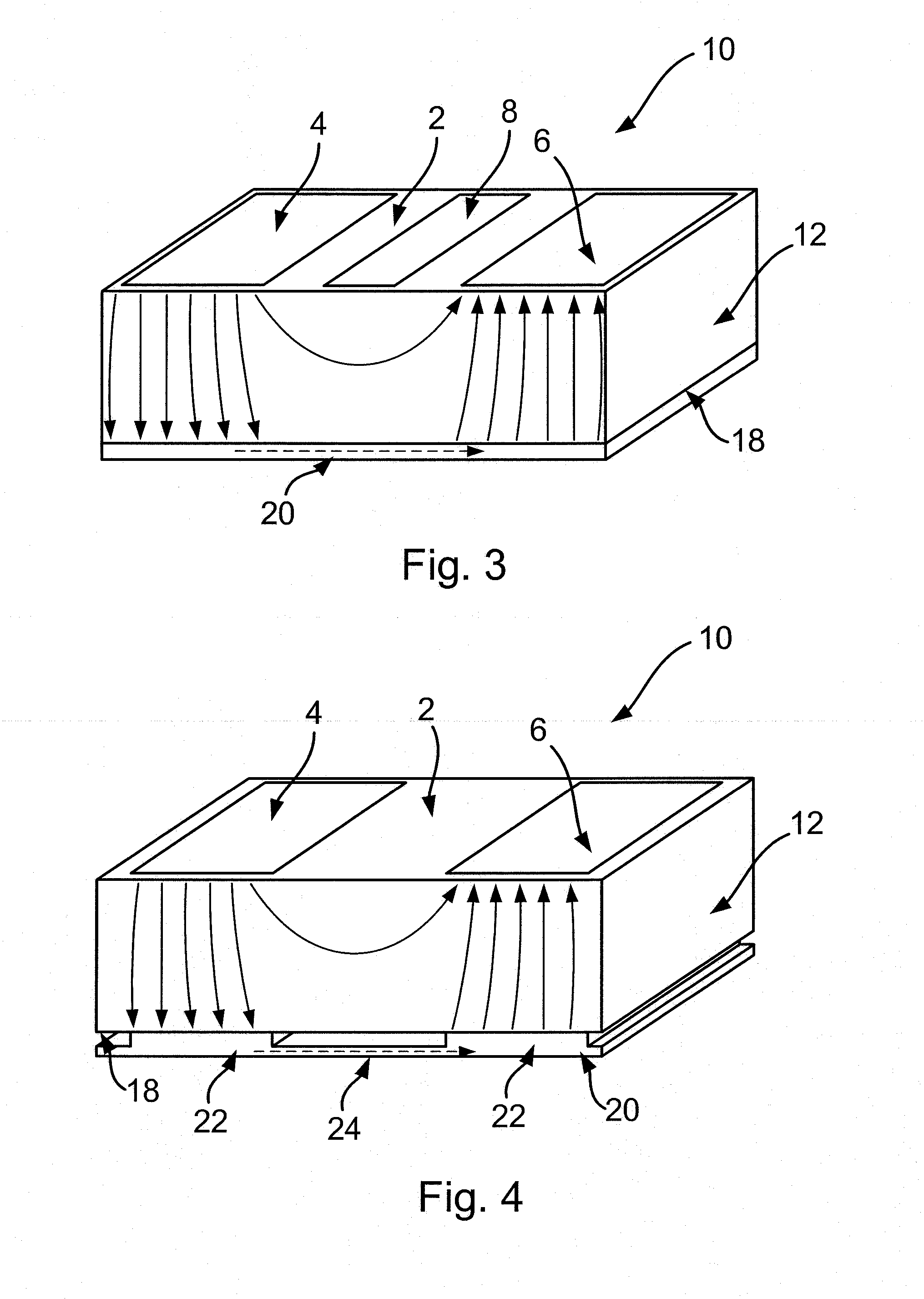
[0046]FIG. 3 shows a semiconductor device 10 in accordance with this invention. In this embodiment, the device 10 includes a substrate 12 that has a major surface 2 on which are provided a plurality of contacts including a first contact 4, a second contact 6 and also a third contact 8. In this embodiment, the device 10 may be a MOS transistor (for instance, a vertical MOS transistor) in which the first contact 4 is a source contact of the transistor, the second contact 6 is a drain contact of the transistor and the third contact 8 is a gate contact of the transistor. In another example, the device 10 may comprise a bipolar transistor in which the first contact 4 is an emitter contact of the transistor, the second contact 6 is a collector contact of the transistor and the third contact 8 is a base contact of the transistor.

[0047]As can be seen from the solid arrows in FIG. 3, the distribution of the current flow within the bulk of the substrate 12 in the device of FIG. 3 is generally...


PUM


Abstract

A semiconductor device and a method of making the same. The device includes a semiconductor substrate provided in a chip-scale package (CSP). The device also includes a plurality of contacts provided on a major surface of the substrate. The device further includes an electrically floating metal layer forming an ohmic contact on a backside of the semiconductor substrate. The device is operable to conduct a current that passes through the substrate from a first of said plurality of contacts to a second of said plurality of contacts via the metal layer on the backside.

Description

FIELD OF THE INVENTION[0001]This invention relates to a semiconductor device. In particular, this invention relates to a semiconductor device that can be provided as a chip scale package (CSP).BACKGROUND OF THE INVENTION[0002]Existing discrete semiconductor devices that handle large currents (such as transient voltage surge devices, Schottky diodes, bipolar transistors and vertical MOS devices) generally include electrical contacts on the top and the back of a semiconductor substrate. In such devices, the main current flows between the contact on the top and the contact on the back of the substrate. Accordingly, the current is generally distributed evenly over the whole bulk of the substrate.[0003]When surface-mount device (SMD) packages were introduced, the problem of connecting the top contact to the same plane as the back contact was solved by using bond wires or clips.[0004]With the further trend to miniaturisation, smaller packages are needed. In devices that handle large curre...

Claims


Application Information

Patent Timeline
28 Jul 2016
Publication
US20160218058A1
IPC
H01L23/498; H01L23/532; H01L21/78
CPC
H01L23/49844; H01L21/78; H01L23/53209; H01L23/49811; H01L23/49827; H01L29/401; H01L29/45; H01L21/743
Inventors
PAN, ZHIHAO; HAHN, FRIEDRICH