Semiconductor device structures comprising polycrystalline CVD diamond with improved near-substrate thermal conductivity

a technology of near-substratum thermal conductivity and device structure, which is applied in the direction of basic electric elements, chemical vapor deposition coating, coating, etc., can solve problems such as inability, and achieve good thermal conductivity, high thermal conductivity, and limited phonon scattering

Active Publication Date: 2016-07-07
AKASH SYST INC
View PDF1 Cites 13 Cited by
  • Summary
  • Abstract
  • Description
  • Claims
  • Application Information

AI Technical Summary

Benefits of technology

[0027]The Raman signal parameters as defined above are indicative of good quality polycrystalline CVD diamond material which has a low sp2 carbon content within the diamond nucleation layer. While such Raman signal parameters have previously been achieved in the bulk of thick polycrystalline CVD diamond material, it is more difficult to achieve such parameters in an early growth stage diamond nucleation layer on wide band gap semiconductor substrates. As described in more detail later in this specification, embodiments of the present invention are able to achieve good quality polycrystalline CVD diamond material in the early stages of growth. This is advantageous when growing polycrystalline CVD diamond films on substrates containing wide band gap compound semiconductor layers for heat spreading applications in semiconductor device structures. As previously described, this is...

Problems solved by technology

However, this is not possible when the diamond material is integrated into compound semiconductor devic...

Method used


Image

  • Semiconductor device structures comprising polycrystalline CVD diamond with improved near-substrate thermal conductivity
  • Semiconductor device structures comprising polycrystalline CVD diamond with improved near-substrate thermal conductivity
  • Semiconductor device structures comprising polycrystalline CVD diamond with improved near-substrate thermal conductivity

Examples


Embodiment Construction

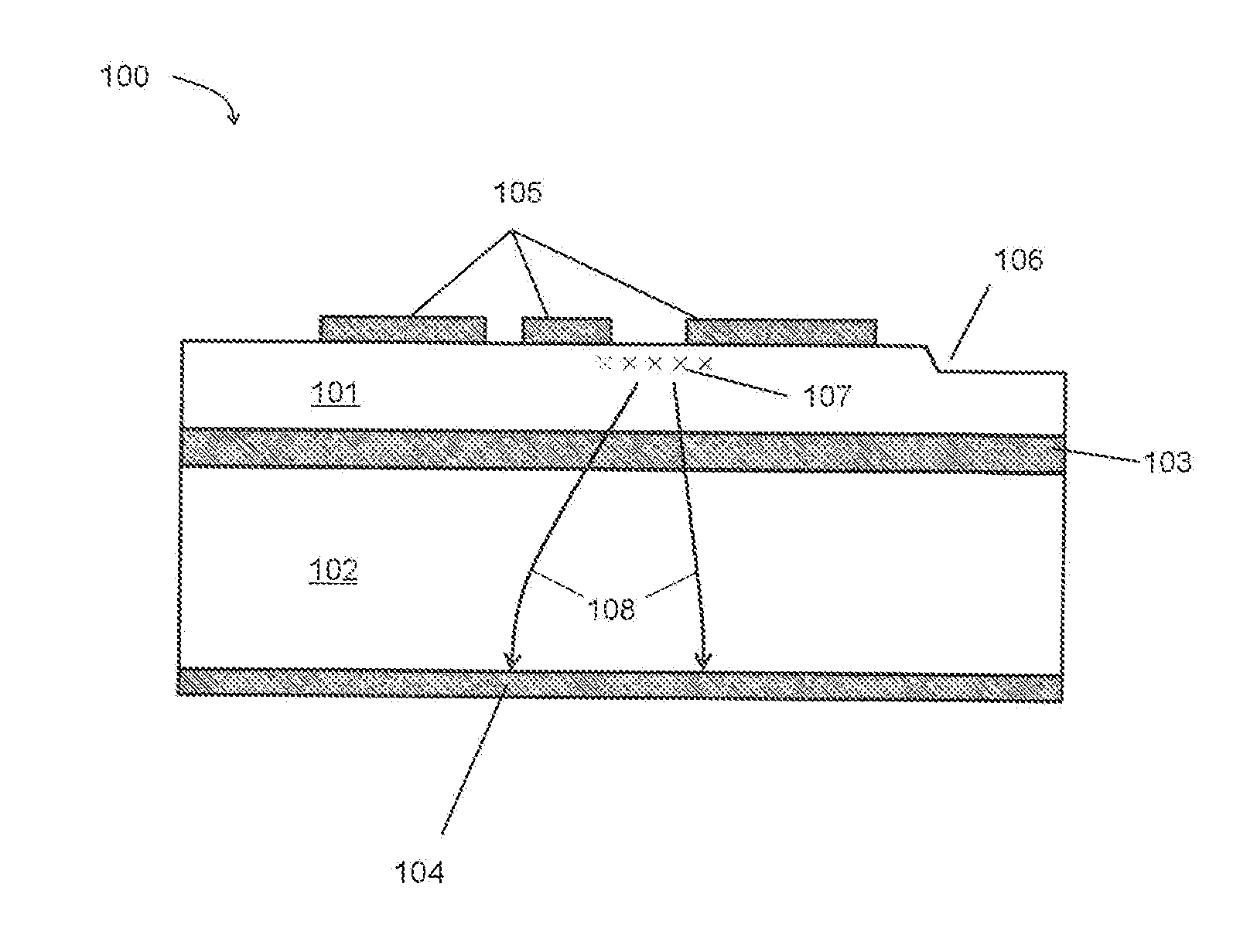
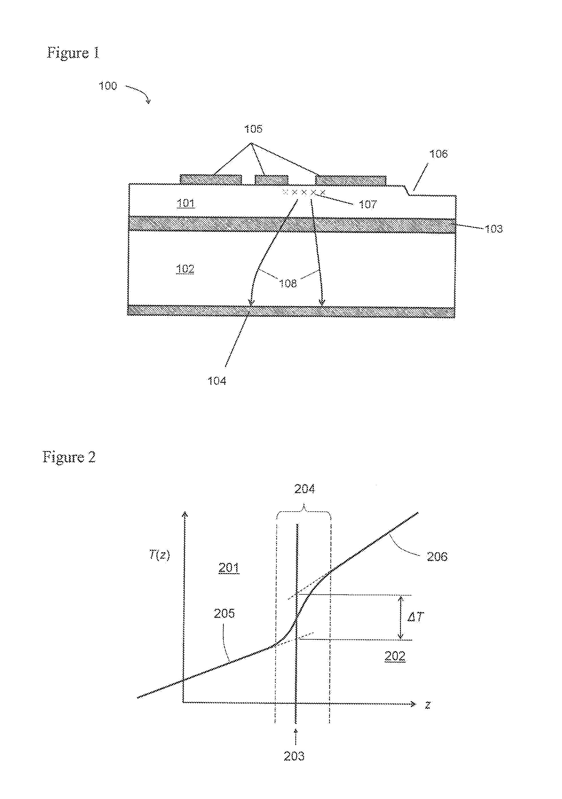
[0049]A number of measurement techniques have been found to be useful in characterizing early growth stage diamond material including Raman spectroscopy, scanning electron microscopy (SEM), and transmission electron microscopy (TEM). These techniques have been found to be useful in analyzing the crystal quality of early growth stage diamond material, sp2 carbon content, thickness of the early growth stage diamond material, and the presence of voids. By analyzing the early growth stage diamond material using these techniques and then adapting seeding, etching, and CVD growth techniques in the early stages of CVD diamond growth it has been found to be possible to provide better quality early growth stage diamond material and thus improve the thermal properties of such material in semiconductor device structures.

[0050]Raman spectroscopy has been found to be a particularly useful technique for measuring sp2 carbon content in localized regions. Raman spectroscopy will typically use a 500...


PUM

PropertyMeasurementUnit
Fractionaaaaaaaaaa
Fractionaaaaaaaaaa
Fractionaaaaaaaaaa

Abstract

A semiconductor device structure comprising:
    • a layer of III-V compound semiconductor material;
    • a layer of polycrystalline CVD diamond material; and
    • an interface region between the layer of III-V compound semiconductor material and the layer of polycrystalline CVD diamond material, the interface region including a diamond nucleation layer of polycrystalline CVD diamond which is formed during an initial nucleation phase of polycrystalline CVD diamond growth over a substrate comprising the layer of III-V compound semiconductor material,
    • wherein the diamond nucleation layer is such that a Raman signal generated by a laser focused on a region comprising the diamond nucleation layer exhibits an sp3 carbon peak at 1332 cm−1 having a full width half-maximum of no more than 5.0 cm−1,
    • wherein the diamond nucleation layer is such that said Raman signal further exhibits one or both of the following characteristics:
      • (i) an sp2 carbon peak at 1550 cm−1 having a height which is no more than 20% of a height of the sp3 carbon peak at 1332 cm−1 after background subtraction when using a Raman excitation source at 633 nm; and
      • (ii) the sp3 carbon peak at 1332 cm−1 is no less than 10% of local background intensity in a Raman spectrum using a Raman excitation source at 785 nm, and
    • wherein an average nucleation density at a nucleation surface of the diamond nucleation layer is no less than 1×108 cm−2 and no more than 1×1012 cm−2.

Description

FIELD OF THE INVENTION[0001]The present invention relates to methods for depositing polycrystalline diamond using chemical-vapor deposition (CVD) on non-diamond substrates with very low near-substrate thermal boundary resistance and semiconductor device structures fabricated using such methods. The invention particularly relates to methods for growing CVD diamond with high thermal conductivity during the initial diamond growth phases. The primary application of this invention is thermal management of high-power electronic and optoelectronic devices.BACKGROUND OF THE INVENTION[0002]Thermal management in semiconductor devices and circuits is a critical design element in any manufacturable and cost-effective electronic and optoelectronic product, such as light generation and electrical signal amplification. The goal of efficient thermal design is to lower the operating temperature of such electronic or optoelectronic device while maximizing performance (power and speed) and reliability...

Claims


Application Information

Patent Timeline
IPC IPC(8): H01L23/373H01L29/20
CPCH01L29/2003H01L23/3732H01L21/02389H01L21/02444H01L21/02513H01L21/02527H01L21/0262H01L21/02658C23C16/0245C23C16/0254C23C16/0272C23C16/27H01L21/02488H01L2924/0002H01L2924/00H01L21/02645H01L21/02115H01L21/0228H01L21/31111
Inventor NASSER-FAILI, FIROOZ
Owner AKASH SYST INC
Why Eureka
Try Eureka