METHOD FOR PRODUCING SiC EPITAXIAL WAFER

a technology of epitaxial wafers and epitaxial wafers, applied in the direction of crystal growth process, crystal growth process, polycrystalline material growth, etc., can solve the problems of deterioration of characteristics, and achieve the effect of reducing the occupation time of the epitaxial wafer manufacturing apparatus, and reducing the time for vacuum baking

Inactive Publication Date: 2016-07-21
SHOWA DENKO KK
View PDF5 Cites 38 Cited by
  • Summary
  • Abstract
  • Description
  • Claims
  • Application Information

AI Technical Summary

Benefits of technology

[0029]According to the method for producing an SiC epitaxial wafer of the present invention, a configuration including the step of vacuum baking a coated carbon-based material member in a dedicated vacuum baking furnace has been adopted. For this reason, although the aging treatment (vacuum baking) of about one week in the epitaxial wafer manufacturing apparatus has been usually required after replacing the coated carbon-based material member, it is possible to eliminate the occupation time of the epitaxial wafer manufacturing apparatus. This makes it possible to utilize all of about one week for production which has usually been a production loss, and the production efficiency can be greatly improved.
[0030]A “dedicated baking furnace” is a furnace prepared, separately from the furnace used in the step of growing an epitaxial film, in order to carry out the baking under predetermined conditions. The expression “dedicated” does not refer to a particular structure of a furnace.
[0031]According to the method for producing an SiC epitaxial wafer of the present invention, a configuration including the step of vacuum baking a coated carbon-based material member at a degree of vacuum of 2.0×10⁻³ Pa or less in a dedicated vacuum baking furnace has been adopted. For this reason, although about one week of vacuum baking has been conventionally required in order to eliminate the incorporated nitrogen from the coated carbon-based material member, the vacuum baking can be carried out within a practical time of about 10 hours by baking at a temperature of 1,400° C. or higher, and it is possible to considerably reduce the time for vacuum baking.
[0032]The shortening of the vacuum baking time makes it possible to utilize a period in which the coated surface of the brand new, coated carbon-based material member is relatively clean. The main cause of the surface defects that are to become killer defects for the SiC devices is the depo

Problems solved by technology

However, these members composed of carbon-based materials typically contain a certain amount of nitrogen.
For this reason, when manufacturing a semiconductor

Method used


Image

  • METHOD FOR PRODUCING SiC EPITAXIAL WAFER
  • METHOD FOR PRODUCING SiC EPITAXIAL WAFER
  • METHOD FOR PRODUCING SiC EPITAXIAL WAFER

Examples


examples

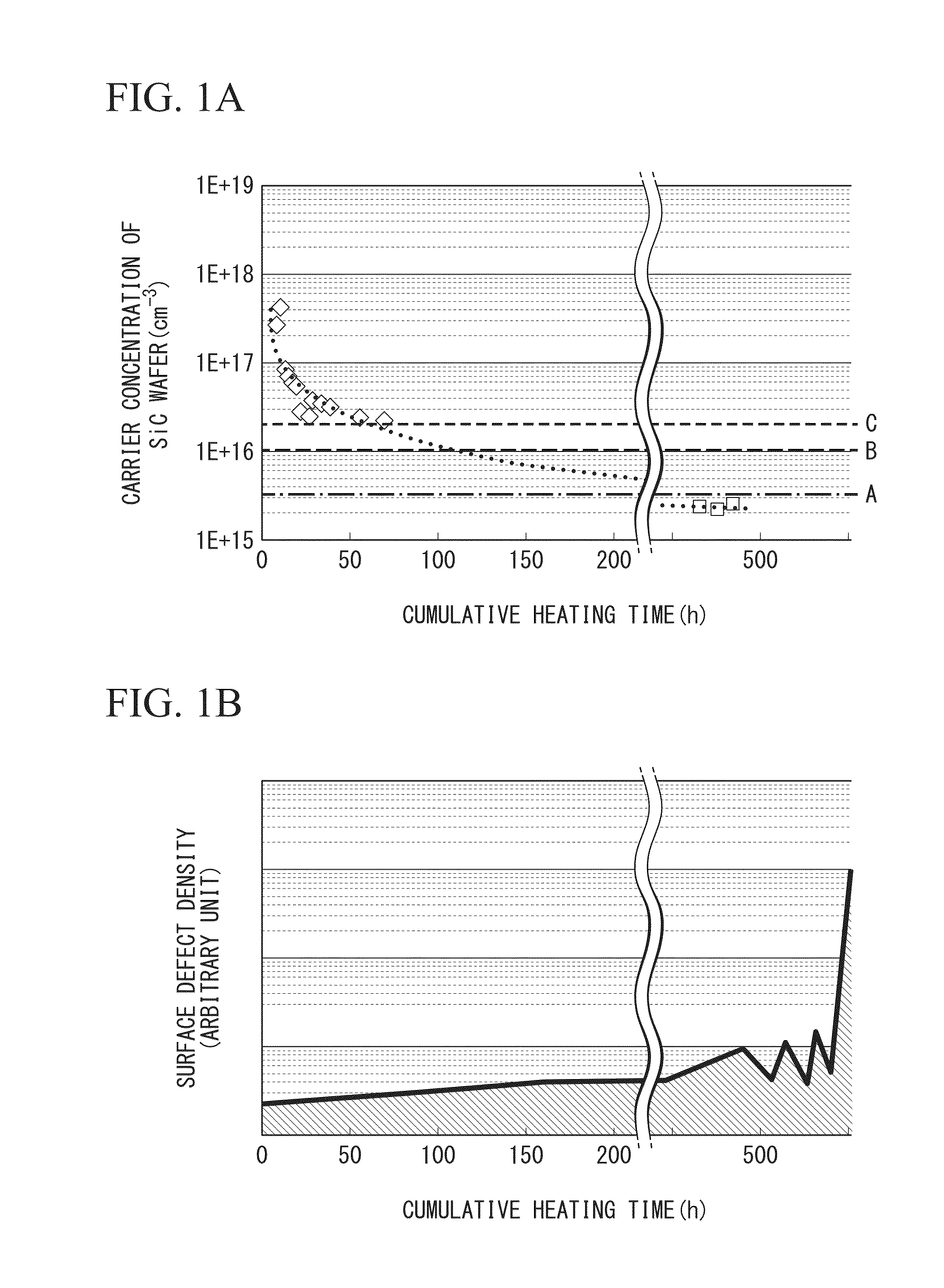
[0098]Hereafter, the effects of the present invention will be described in further detail using examples. Note that the present invention is in no way limited to the examples described below, and can be configured with various modifications, where appropriate, within a range that does not alter the scope and spirit thereof.

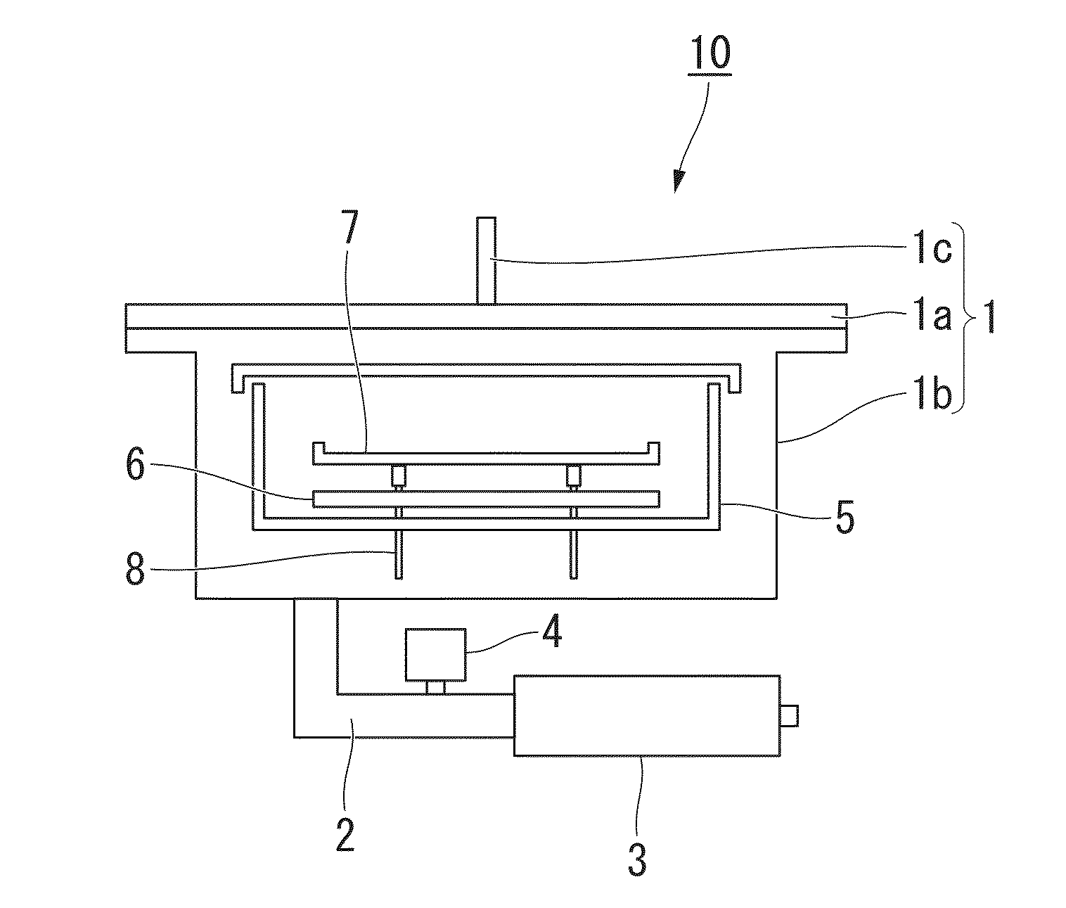
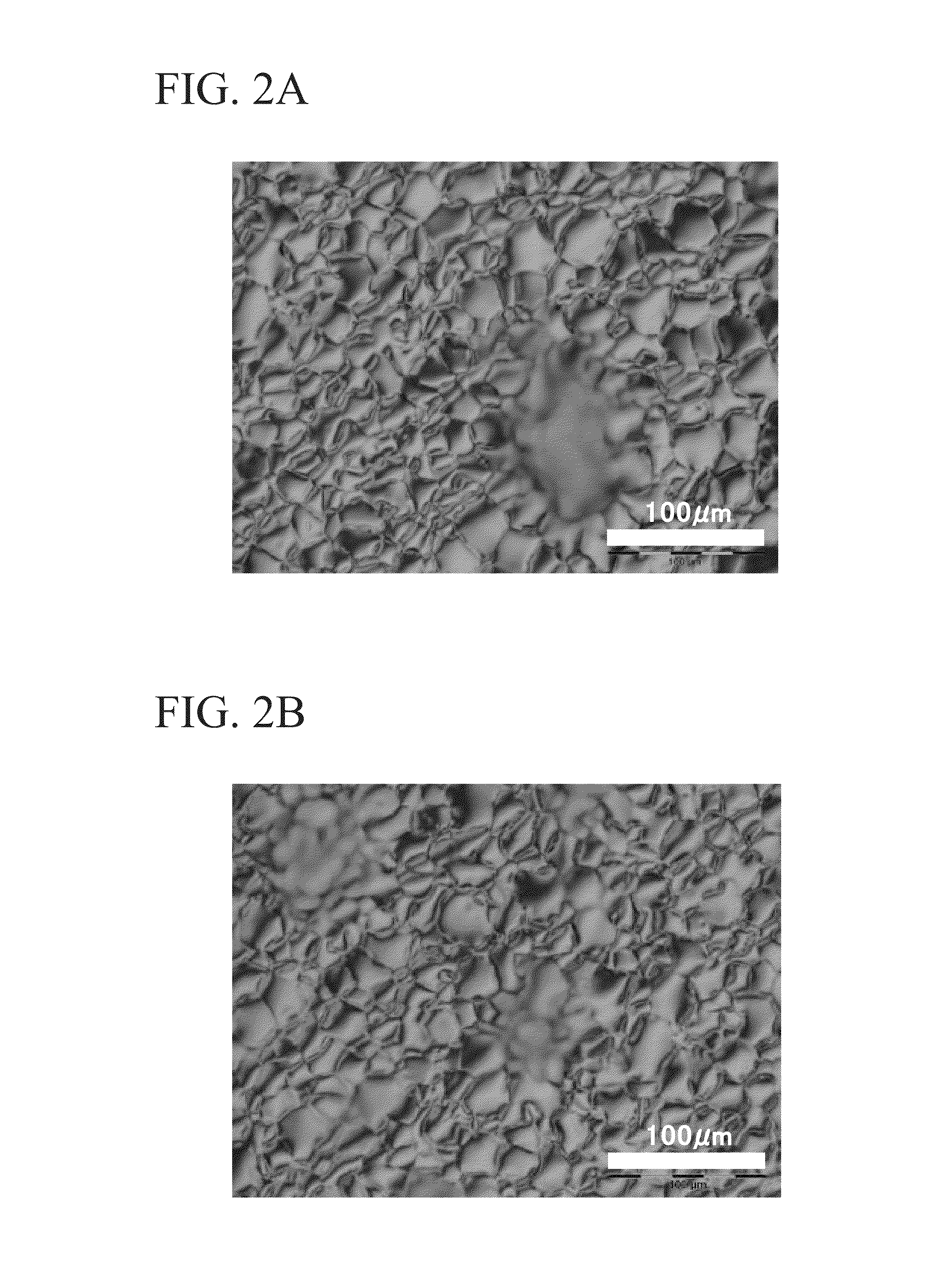
[0099]FIG. 5 shows the transitions of the background carrier concentrations of SiC epitaxial wafers when SiC epitaxial films were formed by actually using a coated carbon-based material member which was subjected to vacuum baking and a carbon-based material member which was not subjected to vacuum baking, respectively. At this time, as an SiC epitaxial wafer manufacturing apparatus, a planetary type SiC-CVD growth apparatus manufactured by AIXTRON SE as shown in the schematic diagram of FIG. 4 was used. In this apparatus, the coated carbon-based material members were mainly composed of four types of members consisted of a susceptor unit (denoted by the reference n...


PUM

PropertyMeasurementUnit
Temperatureaaaaaaaaaa
Pressureaaaaaaaaaa

Abstract

The method for producing an SiC epitaxial wafer according to the present invention includes: a step of vacuum baking a coated carbon-based material member at a degree of vacuum of 2.0×10⁻³ Pa or less in a dedicated vacuum baking furnace; a step of installing the coated carbon-based material member in an epitaxial wafer manufacturing apparatus; and a step of placing an SiC substrate in the epitaxial wafer manufacturing apparatus and epitaxially growing an SiC epitaxial film on the SiC substrate.

Description

TECHNICAL FIELD[0001]The present invention relates to a method for producing an SiC epitaxial wafer. Priority is claimed on Japanese Patent Application No. 2013-183373, filed Sep. 4, 2013, the content of which is incorporated herein by reference.BACKGROUND ART[0002]In general, in a process of manufacturing semiconductors and semiconductor devices and the like, a chemical vapor deposition method has been used as an industrial method for forming a thin film on a substrate. The semiconductors fabricated using this chemical vapor deposition method have been used in many industrial fields.[0003]For example, silicon carbide (SiC) has the superior properties of having a band gap about three times wider, dielectric breakdown field strength about ten times stronger, and thermal conductivity about three times greater than silicon (Si), and is expected to be used in applications such as power devices, high-frequency devices or high-temperature operation devices.[0004]SiC epitaxial wafers are n...

Claims


Application Information

Patent Timeline
IPC IPC(8): C30B25/18H01L21/02C30B29/36
CPCC30B25/186C30B29/36H01L21/0262H01L21/02529H01L21/02378C23C16/325C30B25/20C23C16/4404C30B25/08C30B25/12
Inventor ODAWARA, MICHIYATAJIMA, YUTAKAMUTO, DAISUKEMOMOSE, KENJI
Owner SHOWA DENKO KK
Why Eureka
Try Eureka