Semiconductor device and manufacturing method thereof

a semiconductor device and manufacturing method technology, applied in the direction of transistors, chemical vapor deposition coatings, coatings, etc., can solve the problems of significant affecting transistor characteristics and reliability, difficult control of various steps of manufacturing transistors, and major problems of transistor parasitic capacitance, so as to achieve high-resolution, high-resolution, and high-resolution results

Active Publication Date: 2016-07-28
SEMICON ENERGY LAB CO LTD
View PDF4 Cites 62 Cited by
  • Summary
  • Abstract
  • Description
  • Claims
  • Application Information

AI Technical Summary

Benefits of technology

[0023]According to one embodiment of the present invention, the parasitic capacitance of a transistor can be reduced. Alternatively, a semiconductor device with favorable electrical characteristics can be provided. Alternatively, a highly reliable semiconductor device can be provided. Alternatively, variations in characteristics caused by manufacturing steps of a transistor or a semiconductor device can be reduced. Alternatively, a semiconductor device including an oxide semiconductor layer having few oxygen vacancies can be provided. Alternatively, a semiconductor device that can be manufactured in a simple process can be provided. Alternatively, a semiconductor device with a structure in which the density of interface states in the vicinity of the oxide semiconductor layer can be reduced can be provided. Alternatively, a semiconductor device with low power consumption can be provided. Alternatively, a novel semiconductor device or the like can be provided. Alternatively, a manufacturing method of the semiconductor device can be provided.

Problems solved by technology

In miniaturization of a semiconductor element, the parasitic capacitance of a transistor is a major problem.
It becomes more difficult to control various steps of manufacturing transistors (in particular, film formation, processing, and the like) as the miniaturization advances, and variations in the shapes of the transistors significantly affect transistor characteristics and reliability.

Method used


Image

  • Semiconductor device and manufacturing method thereof
  • Semiconductor device and manufacturing method thereof
  • Semiconductor device and manufacturing method thereof

Examples


embodiment 1

[0118]In this embodiment, a semiconductor device of one embodiment of the present invention and a manufacturing method of the semiconductor device are described with reference to drawings.

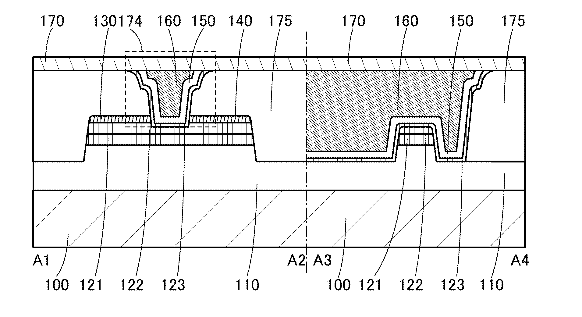
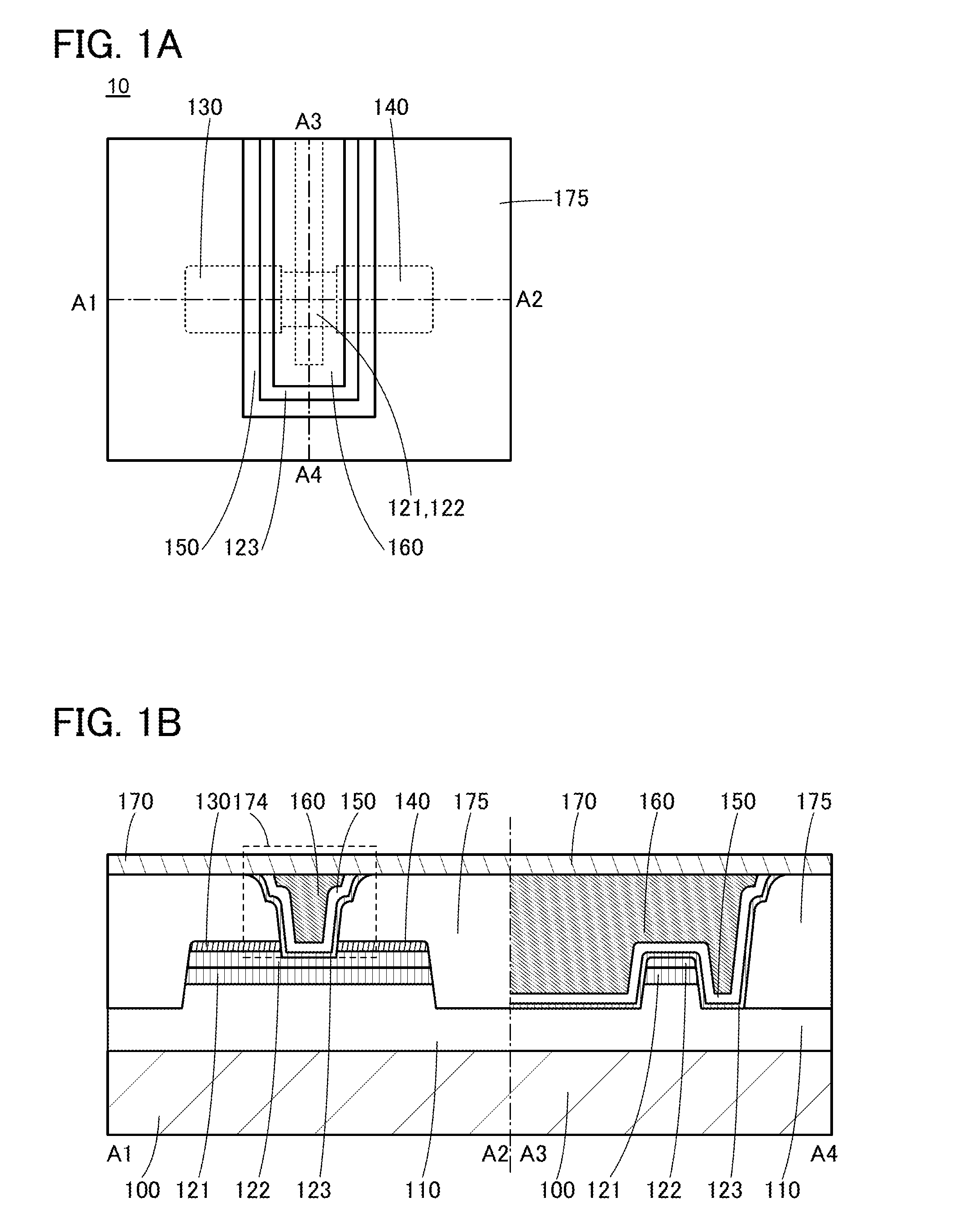
[0119]FIGS. 1A and 1B are a top view and a cross-sectional view which illustrate a transistor 10 of one embodiment of the present invention. FIG. 1A is a top view and FIG. 1B is a cross-sectional view taken along dashed-dotted line A1-A2 and dashed-dotted line A3-A4 in FIG. 1A. In FIG. 1A, some components are scaled up or down or omitted for easy understanding. In some cases, the direction of the dashed-dotted line A1-A2 is referred to as a channel length direction, and the direction of the dashed-dotted line A3-A4 is referred to as a channel width direction.

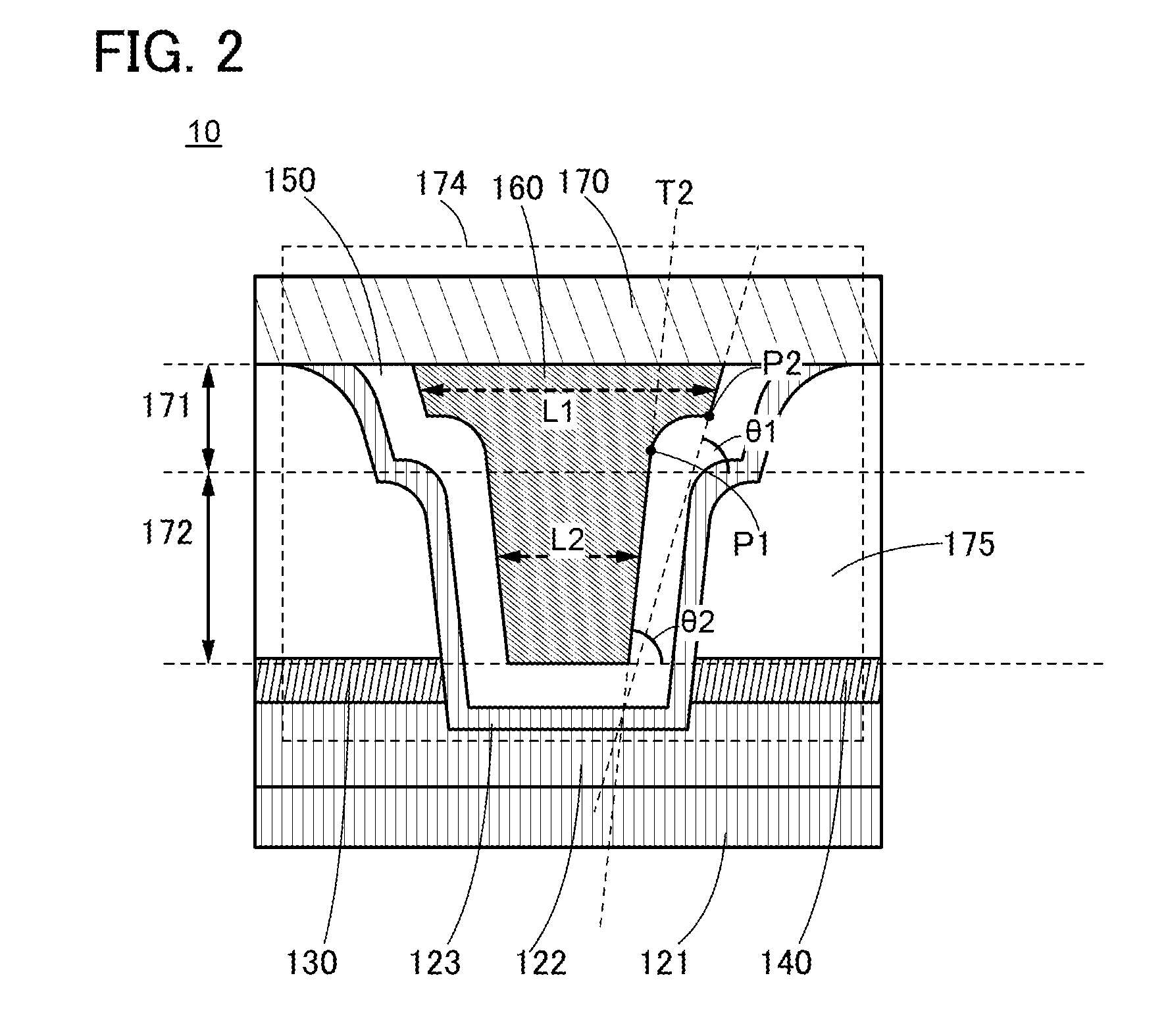
[0120]The transistor 10 includes a substrate 100, an insulating layer 110, an oxide insulating layer 121, an oxide semiconductor layer 122, an oxide insulating layer 123, a source electrode layer 130, a drain electrode layer 140, a gate insulat...

embodiment 2

[0323]In this embodiment, a transistor 13 having a structure which is different from the structures of the transistor 10, the transistor 11, and the transistor 12 described in Embodiment 1 and a method for manufacturing the transistor 13 will be described.

[0324]FIGS. 16A and 16B are a top view and a cross-sectional view of the transistor 13 of one embodiment of the present invention. FIG. 16A is a top view and FIG. 16B is a cross-sectional view taken along dashed-dotted line A1-A2 and dashed-dotted line A3-A4 in FIG. 16A. In FIG. 16A, some components are scaled up or down in size or omitted for easy understanding. In addition, the direction of dashed-dotted line A1-A2 and the direction of dashed-dotted line A3-A4 are sometimes referred to as a channel length direction and a channel width direction, respectively.

[0325]The transistor 13 is different from the transistor 10 in that in the groove portion 174, the end portions of the bottom surface of the insulating layer 175 protrudes fr...

embodiment 3

Oxide Semiconductor Structure

[0336]The structure of an oxide semiconductor is described in this embodiment.

[0337]An oxide semiconductor is classified into a single crystal oxide semiconductor and a non-single-crystal oxide semiconductor. Examples of a non-single-crystal oxide semiconductor include a c-axis aligned crystalline oxide semiconductor (CAAC-OS), a polycrystalline oxide semiconductor, a nanocrystalline oxide semiconductor (nc-OS), an amorphous-like oxide semiconductor (a-like OS), and an amorphous oxide semiconductor.

[0338]From another perspective, an oxide semiconductor is classified into an amorphous oxide semiconductor and a crystalline oxide semiconductor. Examples of a crystalline oxide semiconductor include a single crystal oxide semiconductor, a CAAC-OS, a polycrystalline oxide semiconductor, and an nc-OS.

[0339]It is known that an amorphous structure is generally defined as being metastable and unfixed, and being isotropic and having no non-uniform structure. In oth...


PUM

PropertyMeasurementUnit
angleaaaaaaaaaa
angleaaaaaaaaaa
angleaaaaaaaaaa

Abstract

A semiconductor device includes a first oxide insulating layer over a first insulating layer, an oxide semiconductor layer over the first oxide insulating layer, a source electrode layer and a drain electrode layer over the oxide semiconductor layer, a second insulating layer over the source electrode layer and the drain electrode layer, a second oxide insulating layer over the oxide semiconductor layer, a gate insulating layer over the second oxide insulating layer, a gate electrode layer over the gate insulating layer, and a third insulating layer over the second insulating layer, the second oxide insulating layer, the gate insulating layer, and the gate electrode layer. A side surface portion of the second insulating layer is in contact with the second oxide insulating layer. The gate electrode layer includes a first region and a second region. The first region has a width larger than that of the second region.

Description

TECHNICAL FIELD[0001]The present invention relates to an object, a method, or a manufacturing method. In addition, the present invention relates to a process, a machine, manufacture, or a composition of matter. In particular, the present invention relates to, for example, a semiconductor device, a display device, a light-emitting device, a power storage device, an imaging device, a driving method thereof, or a manufacturing method thereof.[0002]In this specification and the like, a semiconductor device generally means a device that can function by utilizing semiconductor characteristics. A transistor and a semiconductor circuit are embodiments of semiconductor devices. In some cases, a memory device, a display device, or an electronic device includes a semiconductor device.BACKGROUND ART[0003]A technique by which a transistor is formed using a semiconductor film formed over a substrate having an insulating surface has been attracting attention. The transistor is used in a wide range...

Claims


Application Information

Patent Timeline
Patent Type & Authority Applications(United States)
IPC IPC(8): H01L29/786H01L21/02H01L21/4757H01L21/475H01L29/66H01L29/06H01L29/423
CPCH01L29/7869H01L29/0649H01L21/02414H01L21/47573H01L21/475H01L29/66969H01L29/78603H01L29/42376H01L21/02554H01L21/02565H01L21/0262H01L21/67207C23C16/40C23C16/45531H01L27/1225H01L29/42384H01L29/78696H01L27/1207H01L29/78618H01L29/42356H01L29/41733
Inventor ASAMI, YOSHINOBUOKAZAKI, YUTAKAOKAMOTO, SATORUSASAGAWA, SHINYA
Owner SEMICON ENERGY LAB CO LTD
Why Eureka
Try Eureka