

Semiconductor device or electronic device including the same
a technology of semiconductor devices and electronic devices, applied in logic circuits, pulse techniques, instruments, etc., can solve the problems of large standby power, increase the standby power of peripheral circuits, and small size and a larger capacity, so as to reduce the power consumption of semiconductor devices and reduce power consumption
- Summary
- Abstract
- Description
- Claims
- Application Information
AI Technical Summary
Benefits of technology
Problems solved by technology
Method used
Image

Examples
embodiment 1
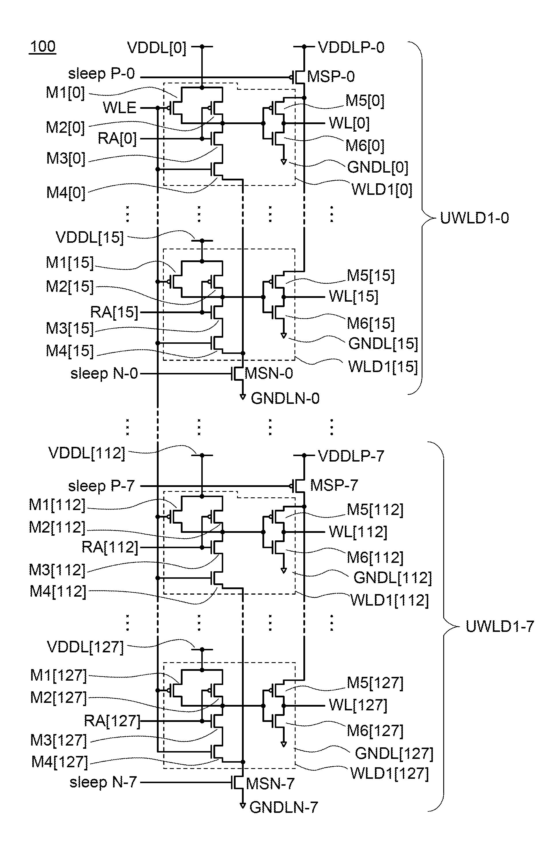
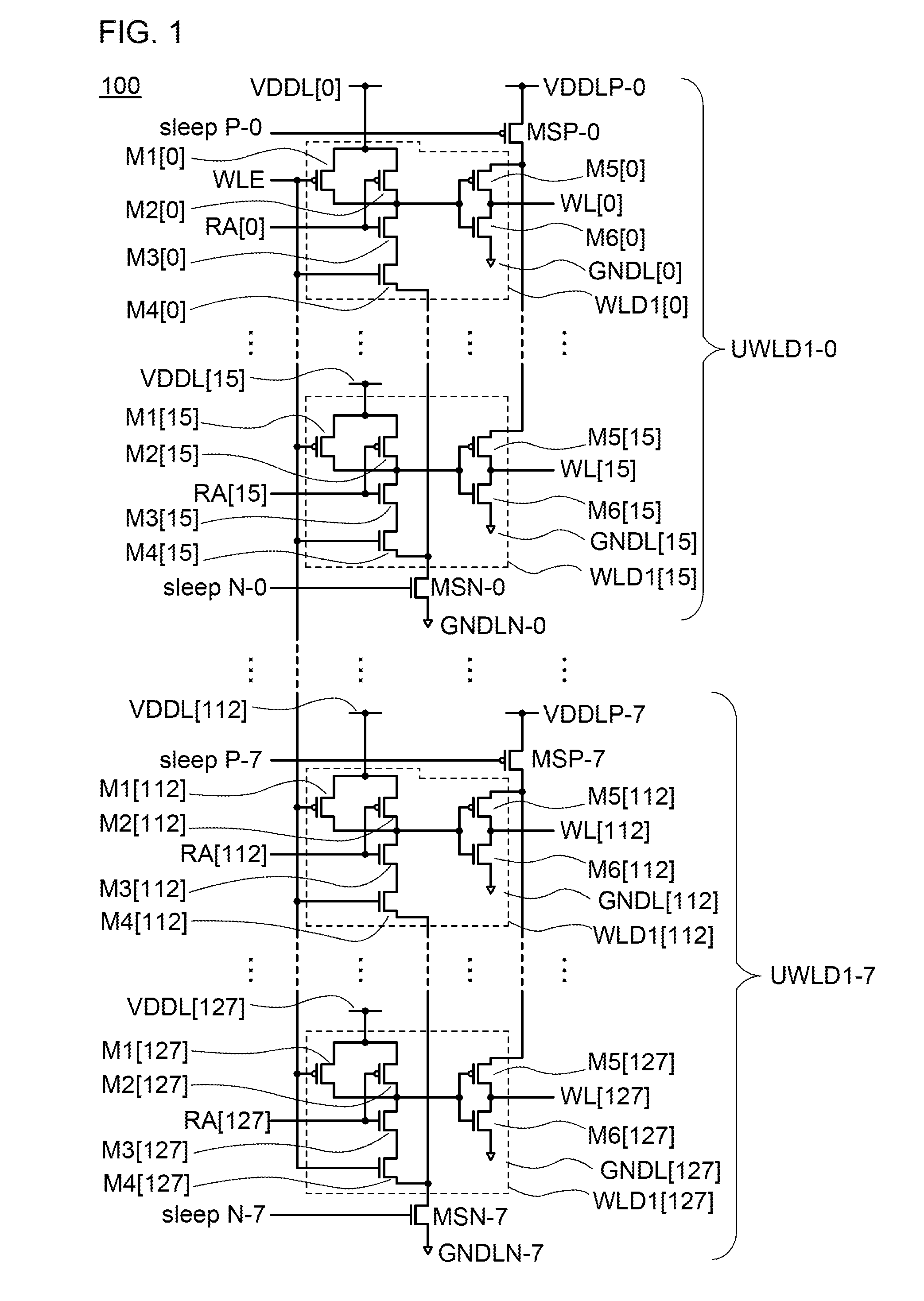
[0093]Described in this embodiment is a structure example of a circuit of a semiconductor device according to one embodiment of the present invention.
[0094]First, a structure example of a word line driver circuit electrically connected to a row of memory cells in a memory cell array of this embodiment will be described.
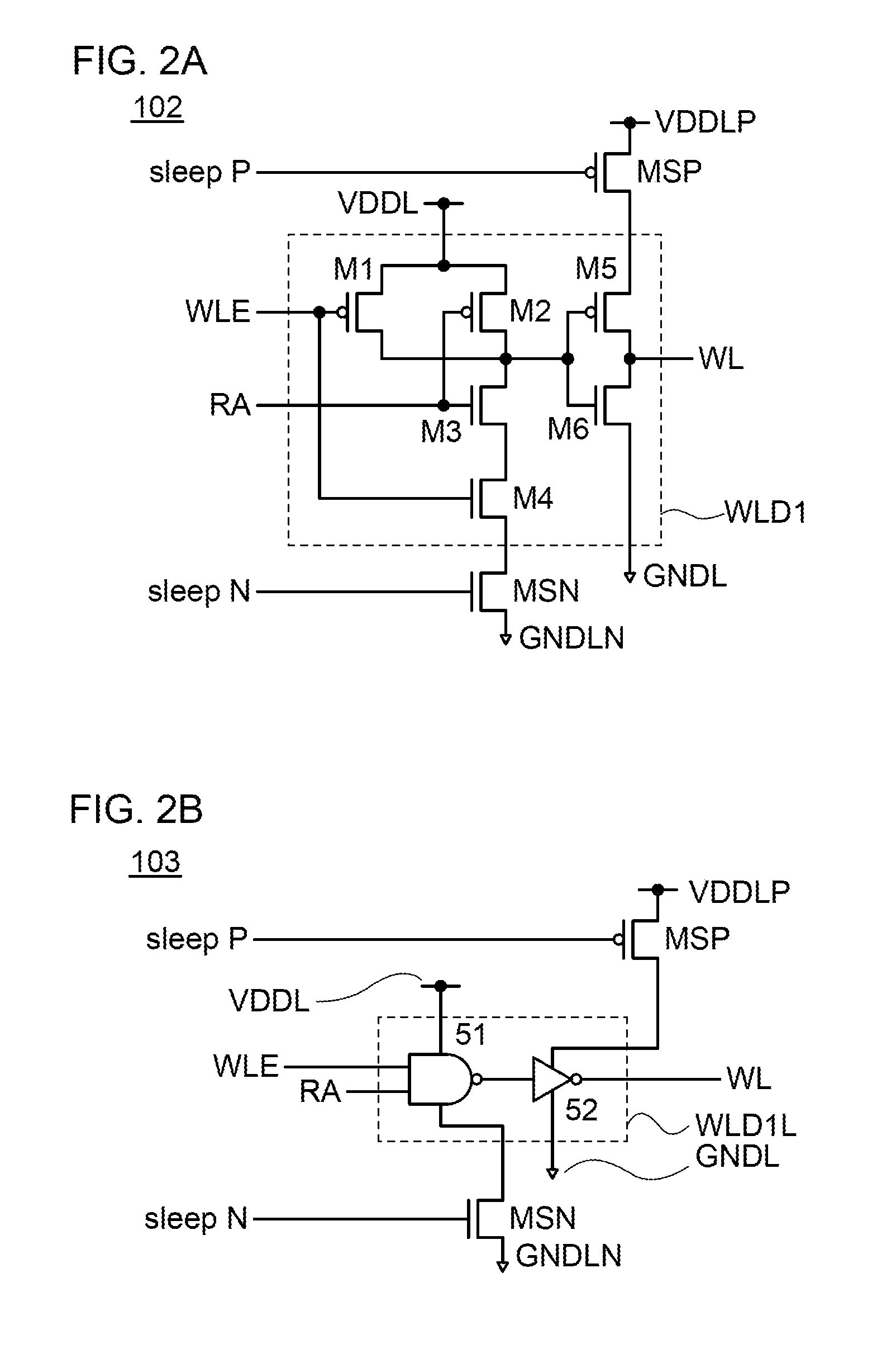
[0095]FIG. 2A shows a structure example of a word line driver circuit. A word line driver circuit 102 includes a transistor MSP, a transistor MSN, and a circuit WLD1. The circuit WLD1 (in this specification, also referred to as a unit word line driver) includes transistors M1 to M6. The transistors MSP, M1, M2, and M5 are p-channel transistors, and the transistors MSN, M3, M4, and M6 are n-channel transistors.
[0096]A gate of the transistor M1 is electrically connected to a gate of the transistor M4 and a wiring WLE. One of a source and a drain of the transistor M1 is electrically connected to one of a source and a drain of the transistor M2, and the other of the sourc...
embodiment 2
[0143]Described in this embodiment is a structure example of a circuit according to one embodiment of the present invention.
1 of Word Line Driver Circuit>
[0144]First, a structure of a word line driver circuit electrically connected to a row of memory cells in a memory cell array of this embodiment will be described.
[0145]FIG. 9A shows a structure example of a word line driver circuit. A word line driver circuit 122 includes a circuit WLD2 (in this specification, also referred to as a unit word line driver), the transistor MSP, the transistor MSN, the transistors M1 to M3, and the transistors M5 and M6. The transistors M1, M2, and M5 are p-channel transistors, and the transistors M3 and M6 are n-channel transistors.
[0146]The gate of the transistor M1 is electrically connected to the wiring WLE. One of the source and the drain of the transistor M1 is electrically connected to one of the source and the drain of the transistor M2, and the other of the source and the drain of the transis...
embodiment 3
[0191]First, a structure example of a word line driver electrically connected to one row of memory cells in a memory cell array of this embodiment will be described.
[0192]FIG. 17A shows a structure example of a word line driver circuit. A word line driver circuit 142 includes the transistor MSP, the transistor MSN, and the circuit WLD1 (in this embodiment, also referred to as a unit word line driver). The circuit WLD1 includes transistors M1 to M6. The transistors MSP, M1, M2, and M5 are p-channel transistors, and the transistors MSN, M3, M4, and M6 are n-channel transistors.
[0193]The gate of the transistor M1 is electrically connected to the gate of the transistor M4 and the wiring WLE. One of the source and the drain of the transistor M1 is electrically connected to one of the source and the drain of the transistor M2, and the other of the source and the drain of the transistor M1 is electrically connected to the other of the source and the drain of the transistor M2, one of the s...
PUM
 Abstract
Description
Claims
Application Information