Circuit assembly

a technology of circuit assembly and busbar, which is applied in the direction of transportation and packaging, printed circuit non-printed electric components association, and final product manufacturing, etc. it can solve the problems of nickel-plated terminal sections of busbars inevitably having a high hardness, the adhesive layer cannot be maintained, and the degree of freedom of selection for plating of busbars cannot be achieved. , the effect of improving the degree of freedom of selection for busbar plating and improving the insulation property of busbar circuit units

Active Publication Date: 2016-08-11
SUMITOMO WIRING SYST LTD
View PDF6 Cites 11 Cited by
  • Summary
  • Abstract
  • Description
  • Claims
  • Application Information

AI Technical Summary

Benefits of technology

[0026]According to this aspect, an electrical component can easily be soldered to the printed wiring of the printed circuit board and the busbar of the busbar circuit unit by reflow soldering, achieving simplification of the manufacturing process. Moreover, removal of the printed circuit board from the busbar circuit unit due to a heating temperature in a reflow furnace is advantageously prevented.
[0027]According to the present invention, since the busbars are buried in the insulator layer, and the insulator layer is fixed to the printed circuit board, the...

Problems solved by technology

However, the circuit assembly having the conventional structure has the problem that in the process of mounting the electrical components by soldering, adhesion between the busbars and the printed circuit board with the adhesive layer cannot be maintained.
In this case, there is the risk that due to the melting of the plated layer, the adhesion between the adhesive layer and the busbars is not maintained and the busbars are removed or separated from the printed circuit board.
Although this measure indeed solves the problem that the plated layers of the busbars are melted due to the heating tempera...

Method used


Image

  • Circuit assembly
  • Circuit assembly
  • Circuit assembly

Examples


Embodiment Construction

[0036]Hereinafter, embodiments of the present invention will be described with reference to the drawings.

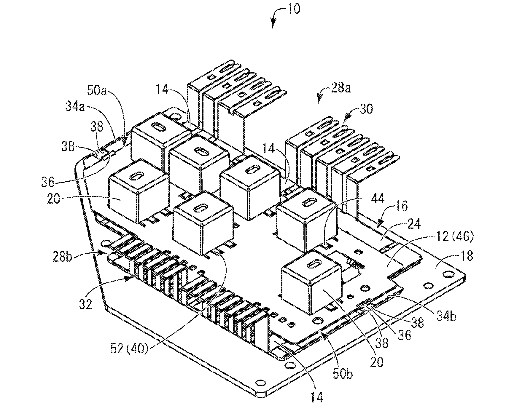
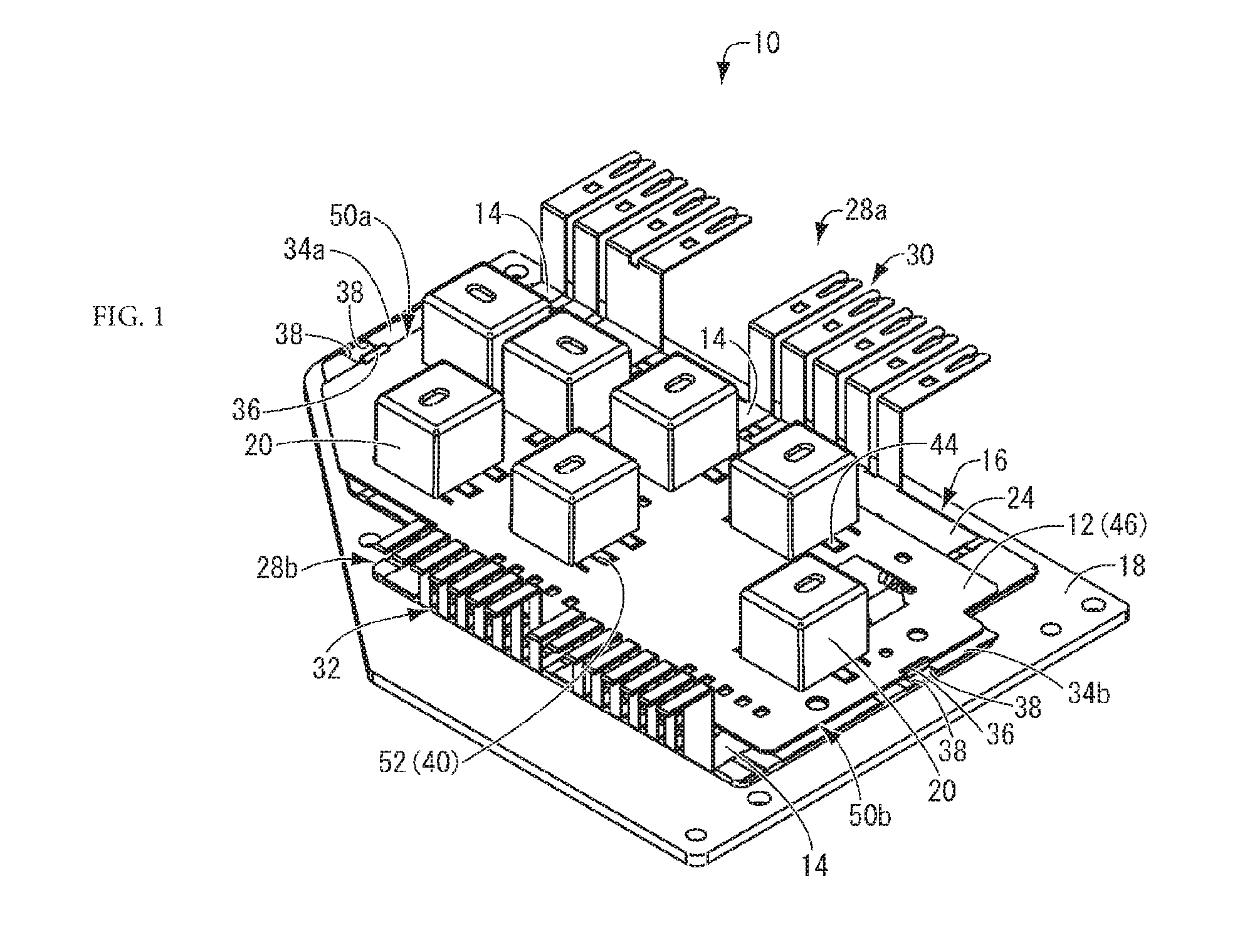
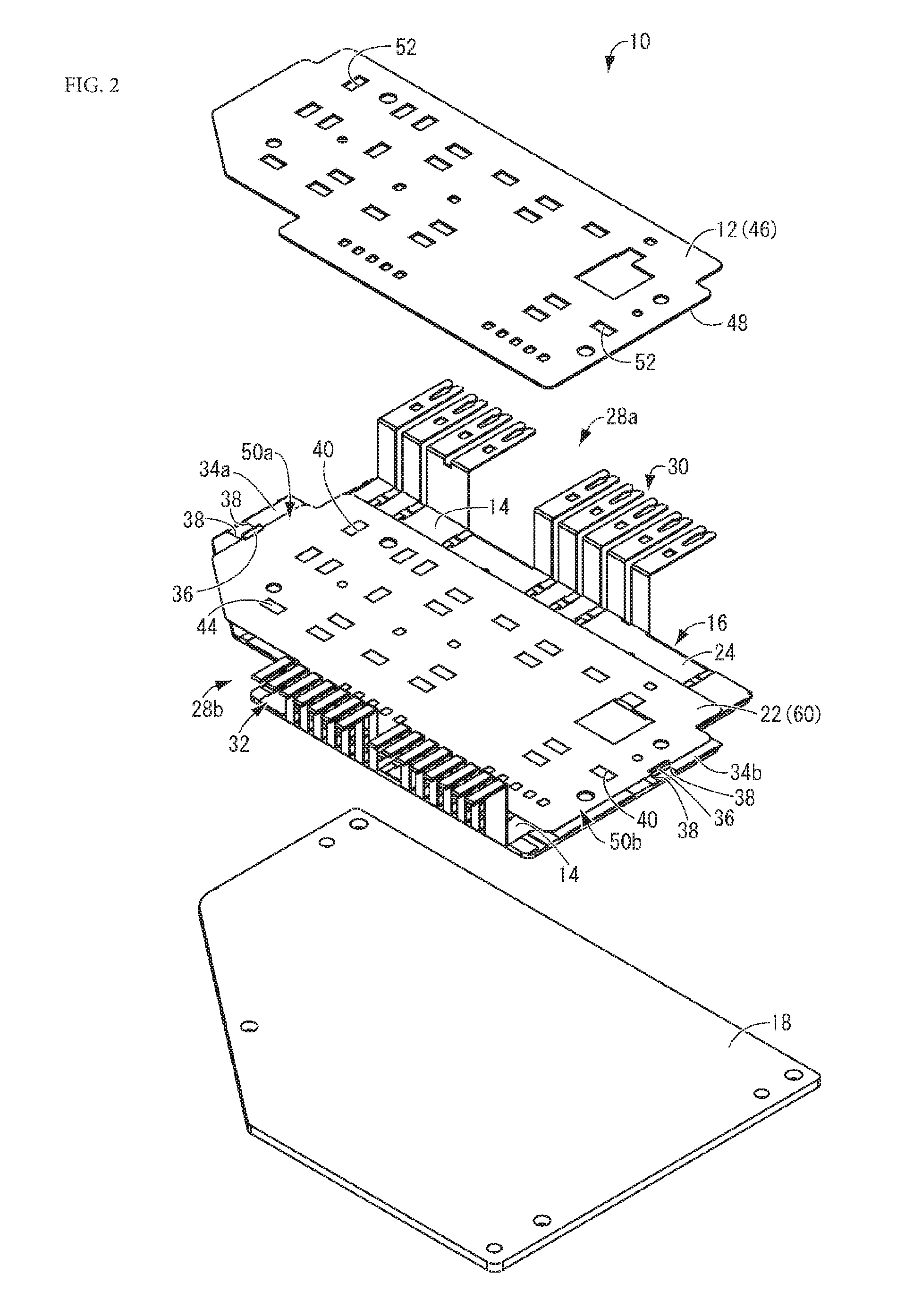
[0037]First, FIGS. 1 to 7 show a circuit assembly 10 serving as an embodiment of the present invention. As shown in FIGS. 1 and 2, the circuit assembly 10 includes a printed circuit board 12 having printed wirings that are not shown, a busbar circuit unit 16 that is constituted by a plurality of busbars 14, and a heatsink 18 that is made of a metal plate. The circuit assembly 10 is constituted by the printed circuit board 12 on which electrical components 20 such as relays are mounted being overlapped with and fixed to the upper side of the busbar circuit unit 16, and the heatsink 18 being directly fixed to the lower side of the busbar circuit unit 16. Note that in the following description, unless otherwise noted, “upper side” refers to the upper side of FIG. 1 on which the printed circuit board 12 is located, and “lower side” refers to the lower side of FIG. 1 on which the heat...


PUM


Abstract

Provided is a circuit assembly having a new structure in which a busbar circuit unit overlapped with a printed circuit board can reliably be fixed regardless of the heating temperature during soldering of an electrical component. In a circuit assembly in which a busbar circuit unit is overlapped with and fixed to a printed circuit board, the busbar circuit unit is configured as one piece by busbars being buried between insulator layers, and a section of the busbars is exposed via a through-hole of the insulator layer. The insulator layer of the busbar circuit unit is overlapped with the printed circuit board and is fixed thereto via fixing means, and terminal sections of an electrical component are soldered to and mounted on the exposed section of the busbar circuit unit and a printed wiring of the printed circuit board.

Description

CROSS-REFERENCE TO RELATED APPLICATIONS[0001]This application is the U.S. national stage of PCT / JP2014 / 073241 filed Sep. 3, 2014, which claims priority of Japanese Patent Application No. JP2013-196764 filed Sep. 24, 2013.FIELD OF THE INVENTION[0002]The present invention relates to a circuit assembly in which a busbar circuit unit constituted by a plurality of busbars is overlapped with and fixed to a printed circuit board.BACKGROUND OF THE INVENTION[0003]Conventionally, circuit assemblies that include a composite arrangement of a printed circuit board serving as a control circuit and a busbar circuit unit that is constituted by a plurality of busbars and serves as a large current circuit are known as a circuit assembly that is to be accommodated in an electrical junction box of an automobile. Particularly in recent years, a circuit assembly, as disclosed in JP 2003-164039A, that has a structure in which busbars constituting a busbar circuit unit are directly fixed to a surface of a ...

Claims


Application Information

Patent Timeline
IPC IPC(8): H05K1/02H05K1/18B60R16/023H05K3/34
CPCB60R16/0238H05K1/0263H05K1/181H05K3/0061H05K3/3421H05K3/341H05K2201/10166H05K2201/10272Y02P70/611H05K1/021B60R16/0239H05K2201/09063Y02P70/50
Inventor NAKAMURA, ARINOBU
Owner SUMITOMO WIRING SYST LTD
Why Eureka
Try Eureka