Chip resistor and method for manufacturing the same

Active Publication Date: 2016-08-25
ROHM CO LTD
View PDF10 Cites 16 Cited by
  • Summary
  • Abstract
  • Description
  • Claims
  • Application Information

AI Technical Summary

Benefits of technology

[0010]The present invention has been proposed under the above-described circumstances, and an object thereof is to provide a chip resistor with improved sulfur resistance at low cost and a method for manufacturing the same. Another object of the present

Problems solved by technology

Since silver sulfide is electrically insulative, progress of sulfurization of the internal electrode may cause disconnection of the internal electrode.
Ag—Pd alloy, however, has a disadvantage of being expensive and economically inefficient.
However, when the content of carbon particles

Method used


Image

  • Chip resistor and method for manufacturing the same
  • Chip resistor and method for manufacturing the same
  • Chip resistor and method for manufacturing the same

Examples


first embodiment

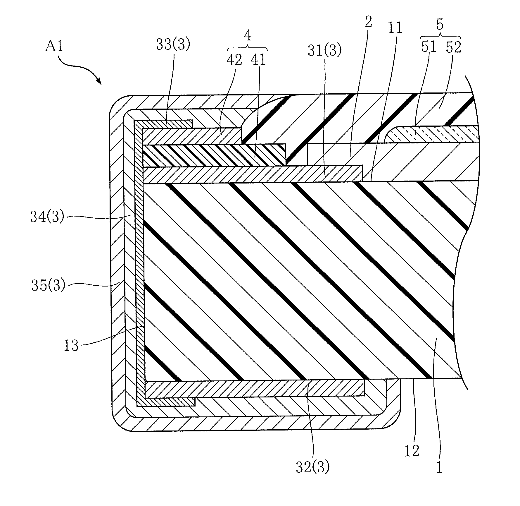
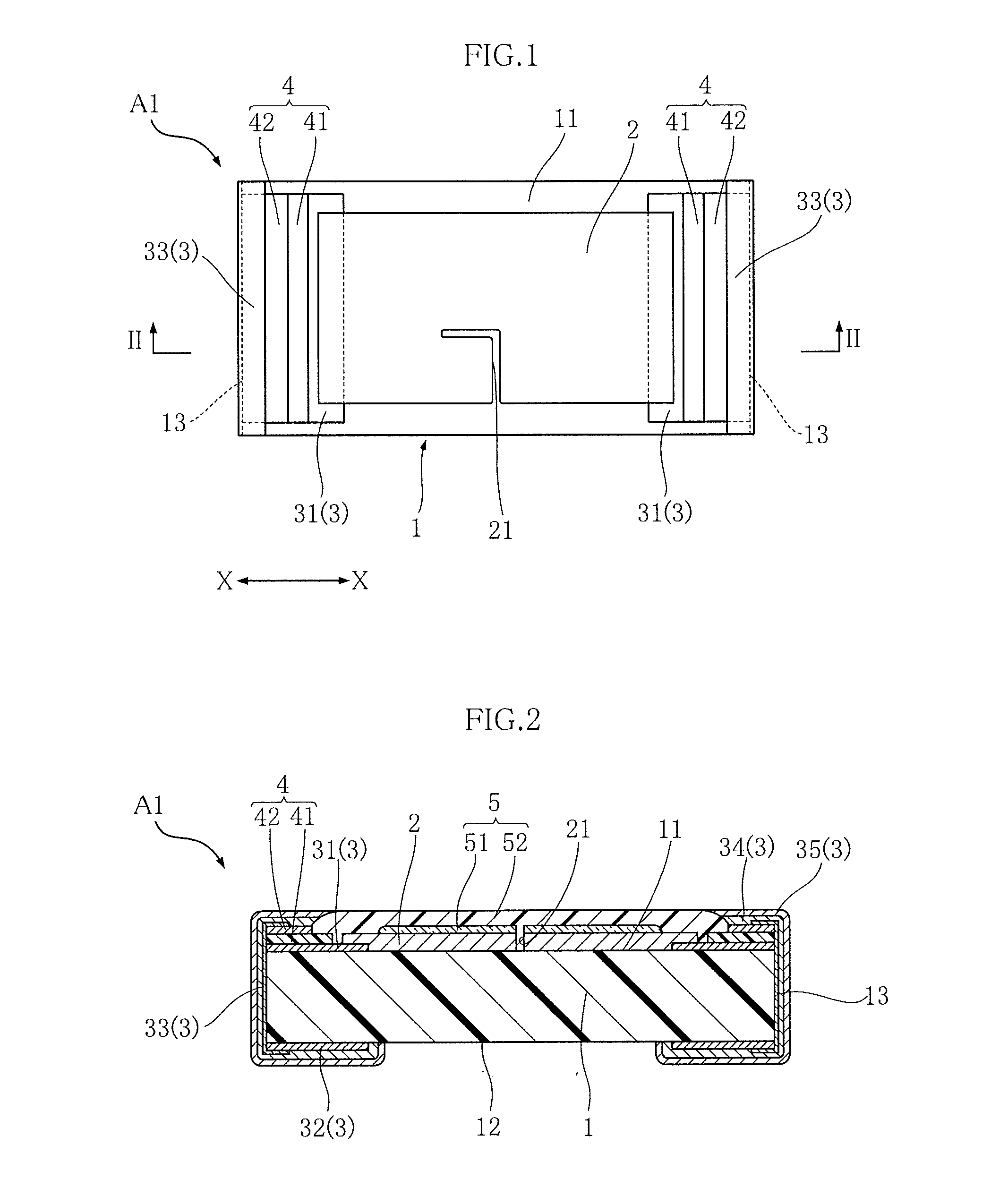
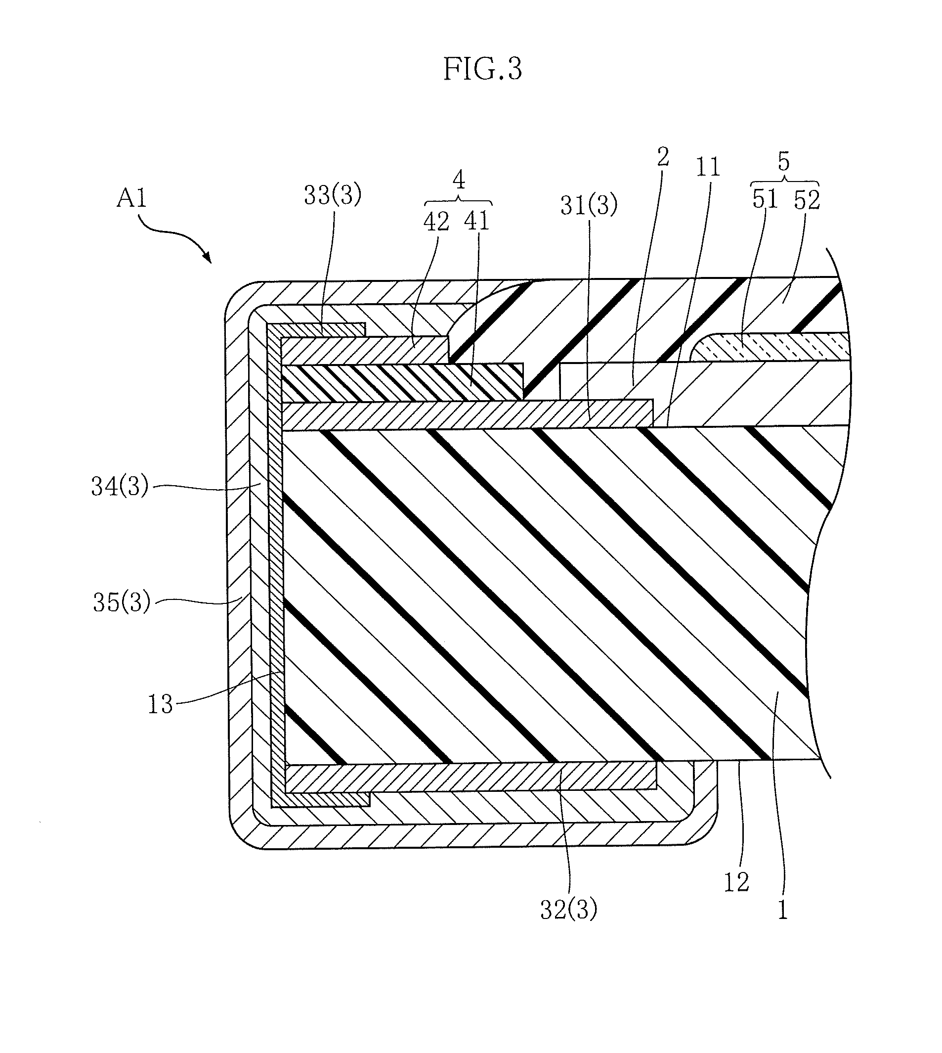
[0112]The following describes a chip resistor A1 according to a first embodiment of the present invention, with reference to FIGS. 1 to 3. FIG. 1 is a plan view showing the chip resistor A1. FIG. 2 is a cross-sectional view along the line II-II in FIG. 1. FIG. 3 is a partial enlarged cross-sectional view showing a part of FIG. 2. For the convenience of understanding, FIG. 1 does not show an intermediate electrode 34, an external electrode 35, or a protection film 5, which are described later.

[0113]The chip resistor A1 shown in these figures is designed to be mounted on a surface of a circuit board in one of various electronic devices. The chip resistor A1 includes a substrate 1, a resistor element 2, electrodes 3, a protective layer 4, and a protective film 5. In the present embodiment, the chip resistor A1 is rectangular in plan view. The chip resistor A1 is a thick film (metal-glaze film) chip resistor.

[0114]As shown in FIGS. 1 and 2, the substrate 1 is a member on which the resis...

second embodiment

[0150]The following describes a chip resistor A2 according to a second embodiment of the present invention, with reference to FIGS. 16 and 17. In these figures, elements that are the same as or similar to the elements of the chip resistor A1 described above are provided with the same reference signs, and descriptions thereof are omitted.

[0151]FIG. 16 is a plan view showing the chip resistor A2. FIG. 17 is a cross-sectional view along the line XVII-XVII in FIG. 16. For the convenience of understanding, FIG. 16 does not show the intermediate electrode 34, the external electrode 35, or the protection film 5. In the present embodiment, the chip resistor A2 is rectangular in plan view.

[0152]The chip resistor A2 differs from the chip resistor A1 in terms of the shape of the resistor element 2 in plan view and the structure of the protective film 5. In the present embodiment, the resistor element 2 has the shape of a serpentine in plan view. The resistor element 2 having the above shape ca...

third embodiment

[0155]The following describes a chip resistor A3 according to a third embodiment of the present invention, with reference to FIGS. 18 to 20. In these figures, elements that are the same as or similar to the elements of the chip resistor A1 described above are provided with the same reference signs, and descriptions thereof are omitted.

[0156]FIG. 18 is a plan view showing the chip resistor A3. FIG. 19 is a cross-sectional view along the line XIX-XIX in FIG. 18. FIG. 20 is a partial enlarged cross-sectional view showing apart of FIG. 19. For the convenience of understanding, FIG. 18 does not show the intermediate electrode 34 or the external electrode 35. As with the chip resistor A1, the chip resistor A3 is a thin-film chip resistor. In the present embodiment, the chip resistor A3 is rectangular in plan view.

[0157]The chip resistor A3 differs from the chip resistor A1 in that the protective layer 4 is omitted, and that the electrodes 3 and the protective film 5 have different structu...


PUM

PropertyMeasurementUnit
Electrical resistanceaaaaaaaaaa
Shapeaaaaaaaaaa
aaaaaaaaaa

Abstract

A chip resistor includes an upper electrode provided on a substrate, a resistor element connected to the upper electrode, and a side electrode connected to the upper electrode. The side electrode, arranged on a side surface of the substrate, has two portions overlapping with the obverse surface and reverse surface of the substrate, respectively. An intermediate electrode covers the side electrode, and an external electrode covers the intermediate electrode. A first protective layer is disposed between the upper electrode and the intermediate electrode, and held in contact with the upper electrode and the side electrode. The first protective layer is more resistant to sulfurization than the upper electrode. A second protective layer is disposed between the first protective layer and intermediate electrode, and held in contact with the first protective layer, side electrode and intermediate electrode.

Description

BACKGROUND OF THE INVENTION[0001]1. Field of the Invention[0002]The present invention relates to chip resistors used in various electronic devices and a method for manufacturing the chip resistors.[0003]2. Description of the Related Art[0004]Conventionally, an internal electrode which is one of the electrodes of a chip resistor may contain silver (Ag). In the case where sulfide gas (such as H2S or SO2) is present in the surrounding environment of an electric device that includes the chip resistor, the silver in the internal electrode may chemically combine with the sulfide gas to generate silver sulfide (Ag2S). Since silver sulfide is electrically insulative, progress of sulfurization of the internal electrode may cause disconnection of the internal electrode.[0005]Japanese Patent Application Publication No. 2013-258292(FIG. 2) discloses a chip resistor including an internal electrode (upper electrode) made of an alloy of silver and palladium (i.e., Ag—Pd alloy). Ag—Pd alloy is exce...

Claims


Application Information

Patent Timeline
IPC IPC(8): H01C1/142C23C14/00H01C1/148
CPCH01C1/142C23C14/0021H01C1/148H01C1/02H01C3/00H01C17/02H01C17/28H01C17/288H01C17/006H01C17/242
Inventor SHINOURA, TAKANORIIMAHASHI, WATARU
Owner ROHM CO LTD
Why Eureka
Try Eureka