

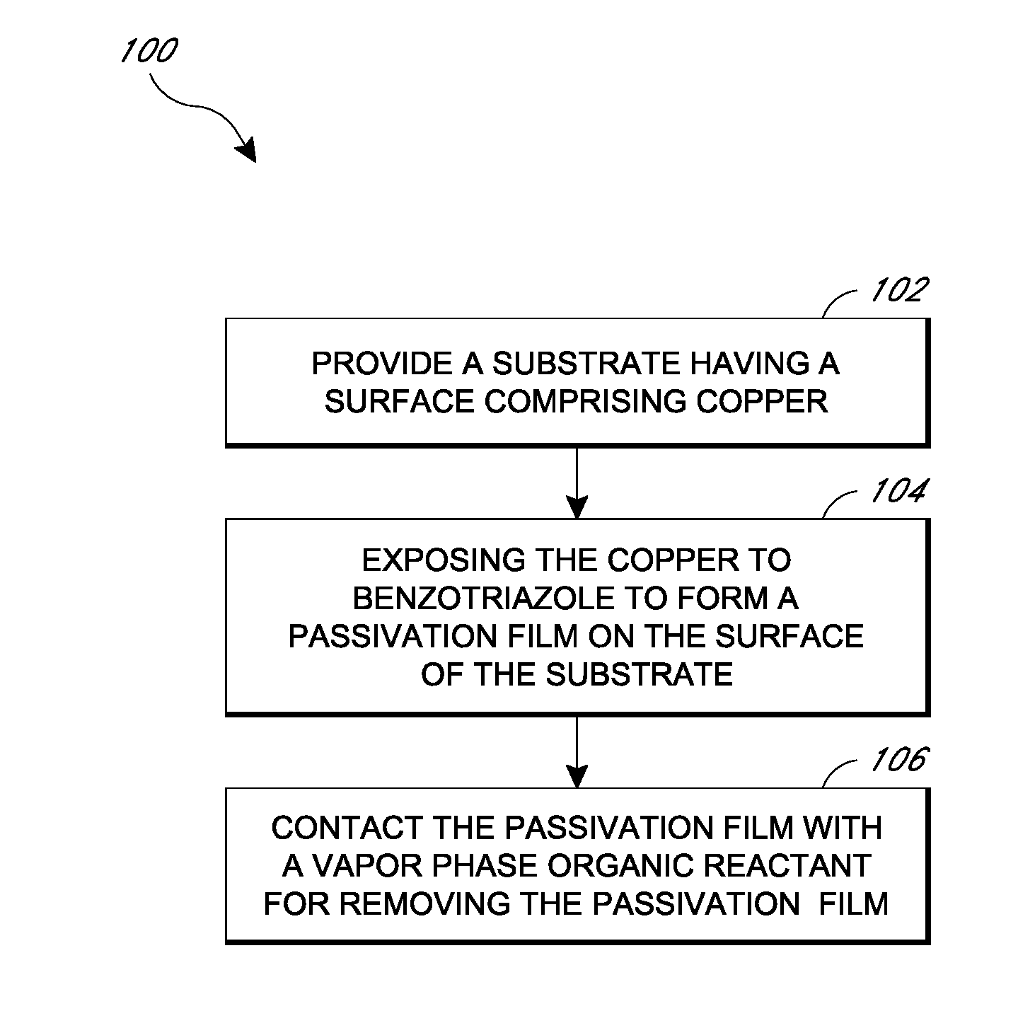
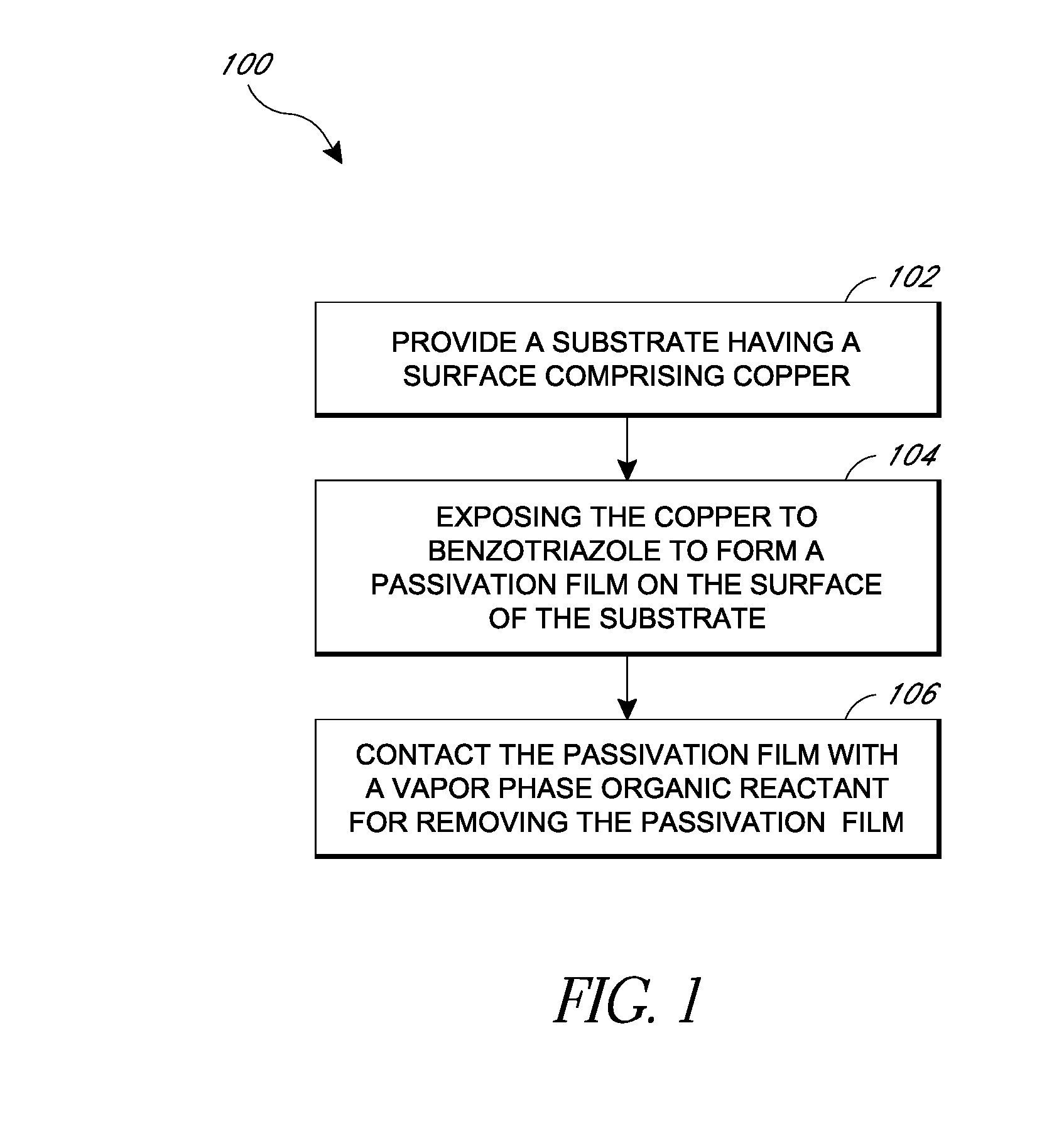
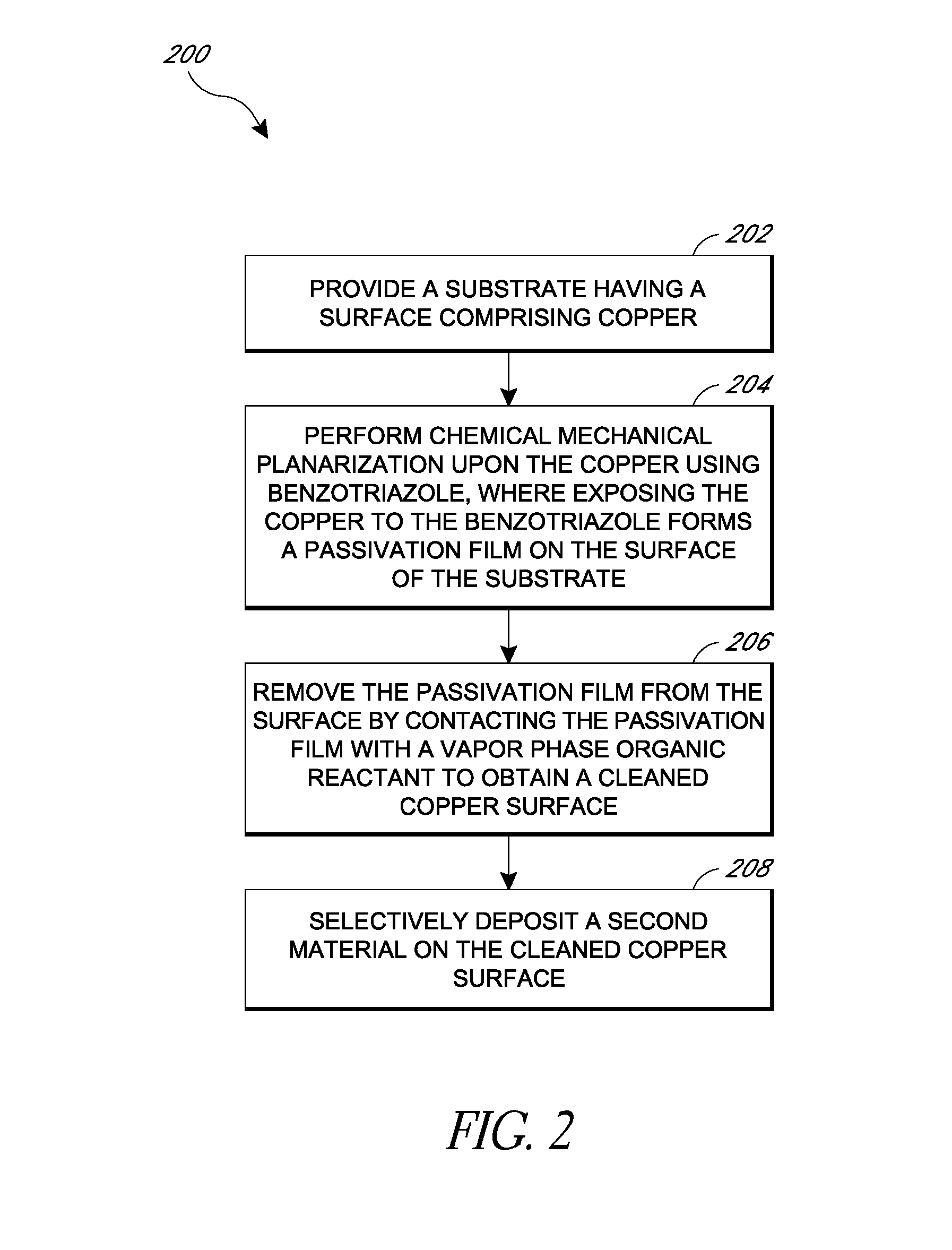
Removal of surface passivation
a surface passivation and passivation film technology, applied in the direction of semiconductor/solid-state device manufacturing, basic electric elements, electric apparatus, etc., can solve the problems of passivation film undesired modification of one or more characteristics of the substrate surface, difficulty in patterning of copper using reactive ion etching (rie),
- Summary
- Abstract
- Description
- Claims
- Application Information
AI Technical Summary
Benefits of technology
Problems solved by technology
Method used
Image

Examples
example
[0097]A substrate comprising a passivation film formed on a surface was subjected to a surface cleaning process, according to one or more embodiments described herein. The passivation film was formed over a copper layer on a surface, due to reaction of the copper layer and benzotriazole. The substrate surface also included a dielectric material (e.g., a dielectric material having a k value of about 2.3, or an extreme low-k material (ELK 2.3 dielectric material)). The cleaning process facilitated removal of the passivation film such that a cleaned copper surface was provided. The cleaned copper surface comprised restored elemental copper. The surface cleaning process included 10 repetitions of contacting the passivation film with a vapor phase reactant, where each repetition had a duration of about 10 s. A purge step was performed following each repetition of contacting the passivation film with a vapor phase reactant. The vapor phase reactant of the surface clean process included fo...
PUM
| Property | Measurement | Unit |
|---|---|---|
| temperature | aaaaa | aaaaa |
| temperature | aaaaa | aaaaa |
| temperature | aaaaa | aaaaa |
Abstract
Description
Claims
Application Information