Display Panel, Manufacturing Method Thereof, and Display Device
a display panel and manufacturing method technology, applied in the direction of semiconductor devices, electrical devices, organic semiconductor devices, etc., can solve the problems of shortened service life of components, damaged pixels, low work function, etc., and achieve the effect of improving the bendability and improving the bendability of the display devi
- Summary
- Abstract
- Description
- Claims
- Application Information
AI Technical Summary
Benefits of technology
Problems solved by technology
Method used
Image
Examples
first embodiment
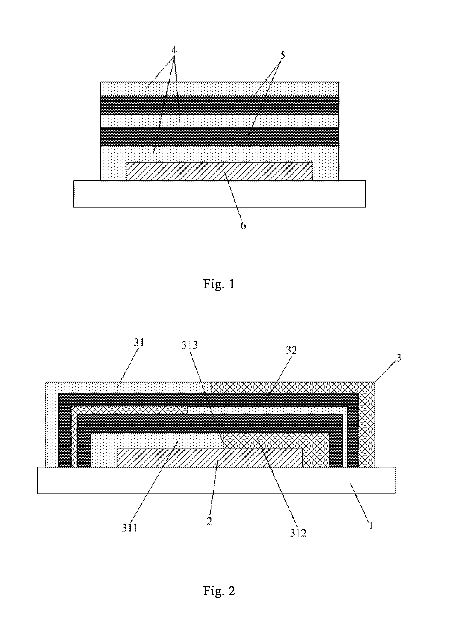
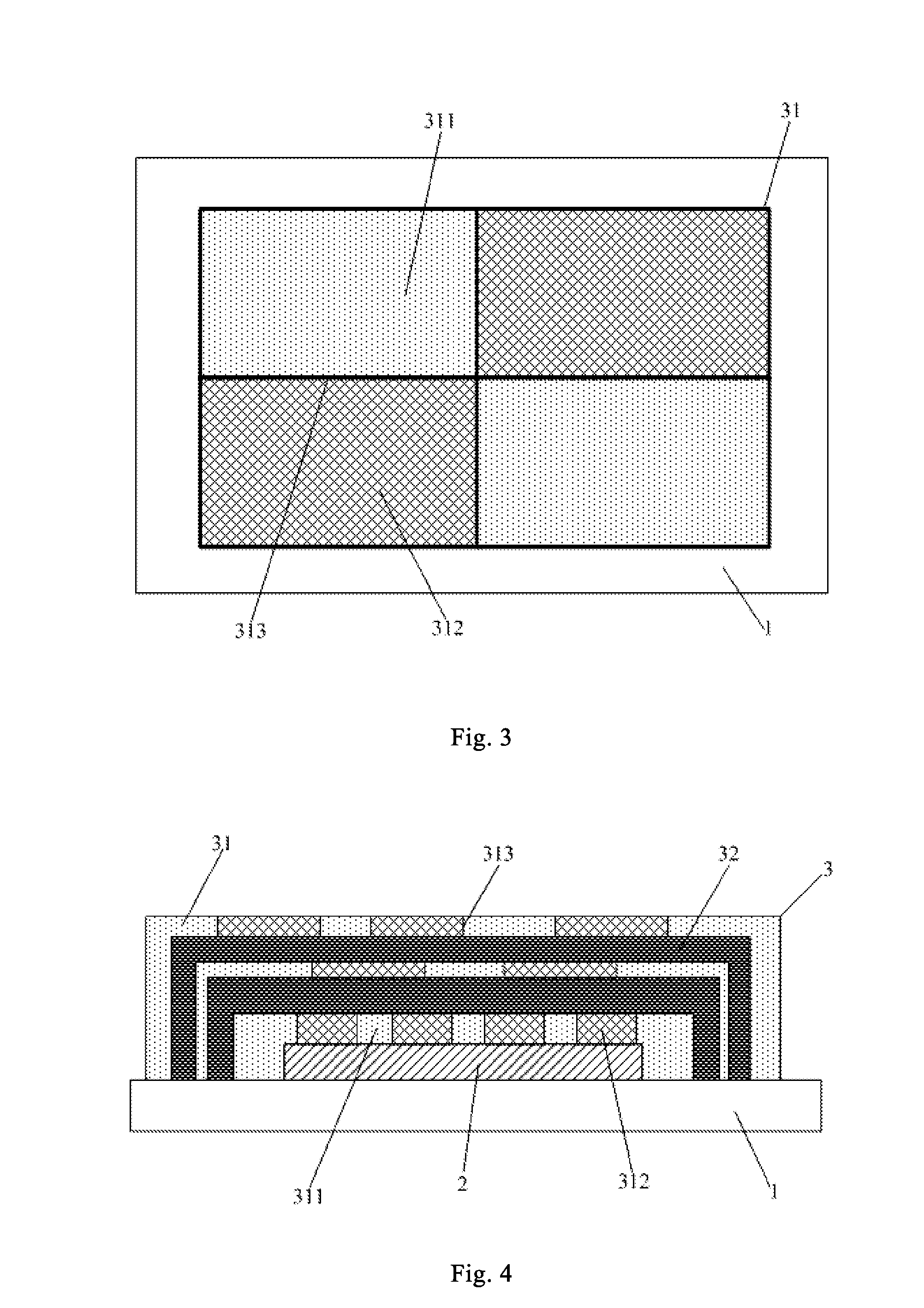
[0041]In this embodiment, the packaging structure 3 includes three first water blocking layers 31 and two planarization layers 32. The display component 2 is an OLED display component, and the display panel with the OLED display component can be bent flexibly.
[0042]In this embodiment, as shown in FIG. 3, in each first water blocking layer 31, the first areas 311 and the second areas 312 are arranged alternately in both row and column directions. Specifically, one first area 311 and one second area 312 are included in the row direction, and also, one first area 311 and one second area 312 are included in the column direction. With such configuration, when the display panel is bent, stress applied to each first water blocking layer 31 in both row and column directions can be better dispersed, so that the stress applied to the entire first water blocking layer 31 becomes uniform, which in turn leads to that the entire first blocking layer 31 can hardly crack at any position, thereby im...
second embodiment
[0070]This embodiment provides a display panel, and as shown in FIGS. 4 and 5, in each first water blocking layer 31, the first areas 311 and the second areas 312 are arranged alternately in both row and column directions. What differs from the first embodiment is in that, a plurality of first areas 311 and a plurality of second areas 312 are included in both row and column directions.
[0071]It could be understood that, in each first water blocking layer 31, the numbers of the first areas 311 and the second areas 312 included in the row or column direction may be different, as long as the plurality of first areas 311 and the plurality of second areas 312 are arranged alternately, for example, the number of the first areas 311 may be one larger or smaller than the number of the second areas 312. Furthermore, the number of the first areas 311 or second areas 312 included in the row direction may be different from that included in the column direction, the numbers of the first areas 311...
third embodiment
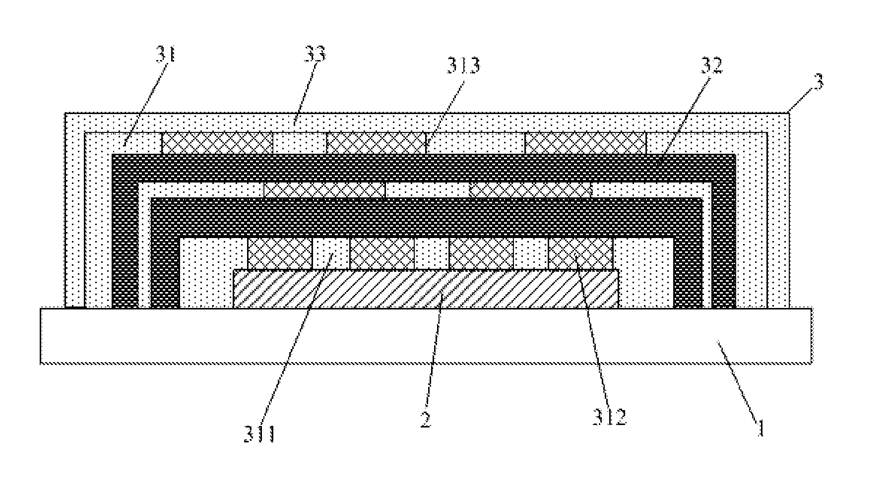
[0074]This embodiment provides a display panel, which differs from the first and second embodiments in that, the packaging structure in this embodiment further includes at least one second water blocking layer, which is stacked above the display component and is made of an inorganic material.
[0075]In this embodiment, as shown in FIG. 6, the packaging structure includes one second water blocking layer 33, which is stacked on the outermost layer above the display component 2 (i.e., is provided as the outermost layer of the packaging structure). Specifically, the second water blocking layer 33 is stacked on the first water blocking layer 31 farthest away from the display component 2.
[0076]Since the second water blocking layer 33 is not divided into first areas and second areas (i.e., the second water blocking layer 33 is an integral film layer), by providing the second water blocking layer 33, water vapor in the external environment can be further prevented from invading into the insid...
PUM
 Abstract
Description
Claims
Application Information


