Method of fabricating MEMS devices using plasma etching and device therefor
- Summary
- Abstract
- Description
- Claims
- Application Information
AI Technical Summary
Benefits of technology
Problems solved by technology
Method used
Image

Examples
Embodiment Construction
[0019]The present invention is directed to MEMS (Micro-Electro-Mechanical-Systems).
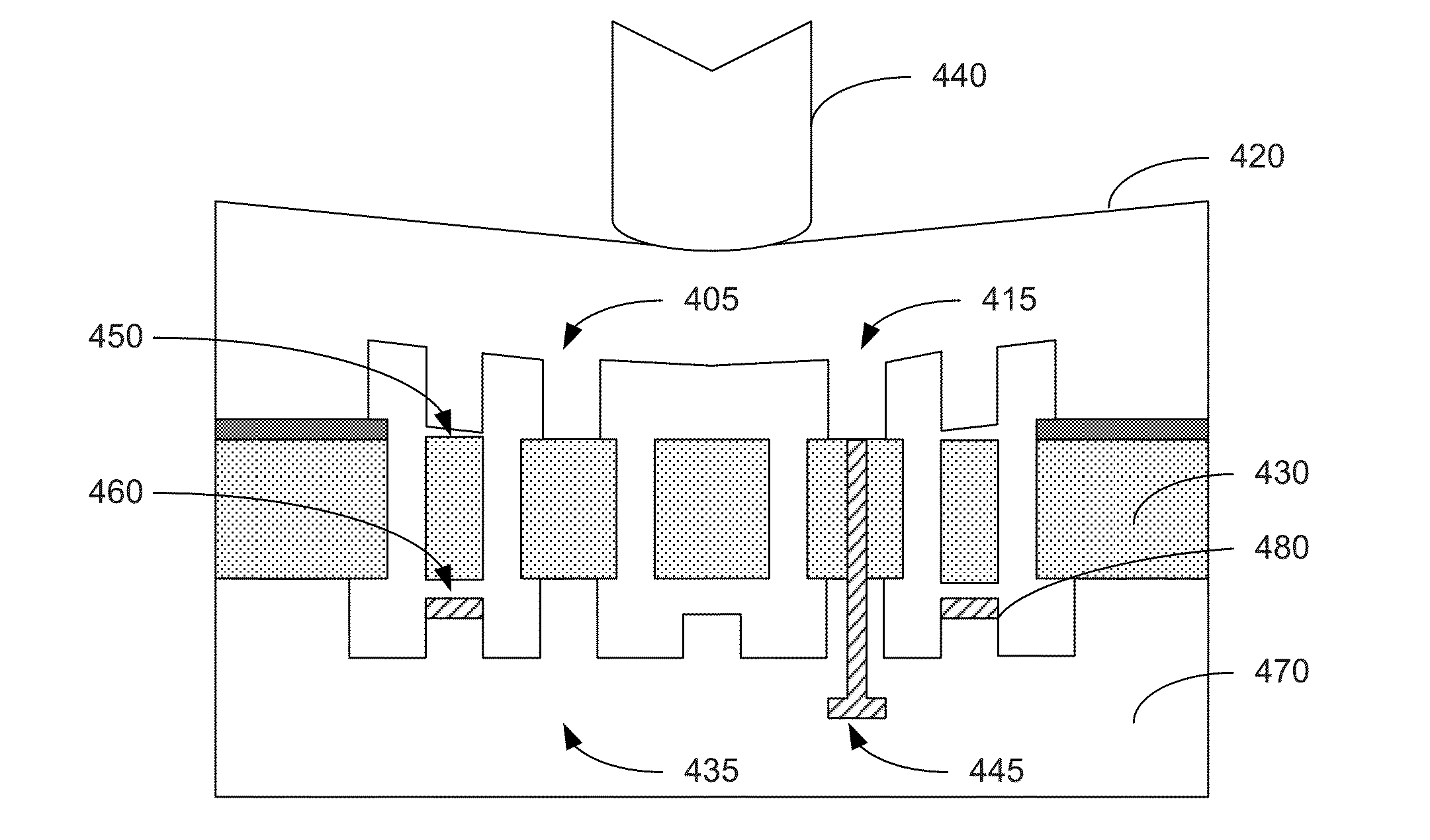
[0020]More specifically, embodiments of the invention provide methods for fabricating an integrated MEMS device, including MEMS sensors and the like, and a resulting device structure. Merely by way of example, the MEMS device can include at least an accelerometer, a gyroscope, a magnetic sensor, a pressure sensor, a microphone, a humidity sensor, a temperature sensor, a chemical sensor, a biosensor, an inertial sensor, and others. But it will be recognized that the invention has a much greater range of applicability.
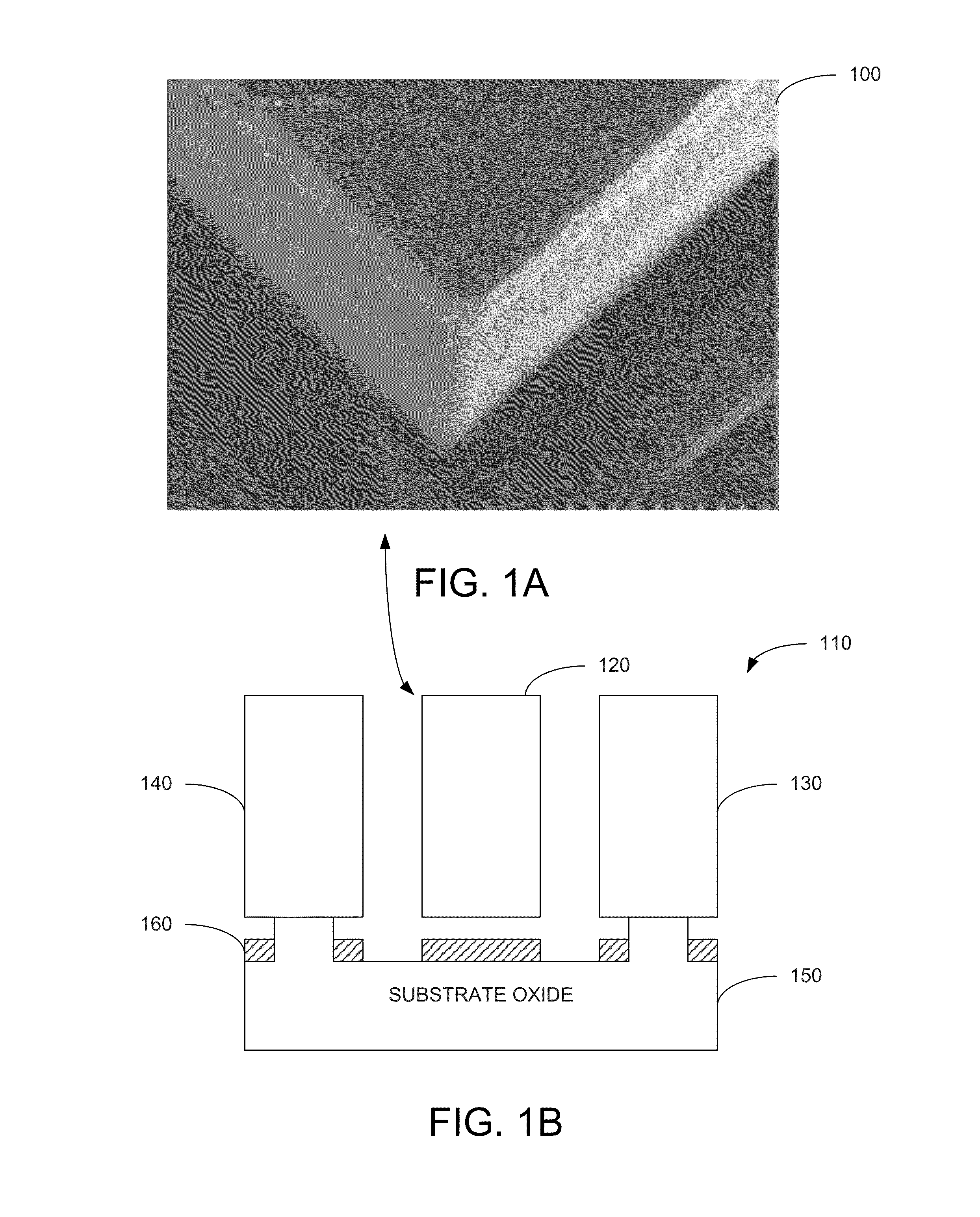
[0021]FIG. 1A shows an SEM (Scanning Electron Microscope) image 100 of a proof mass edge according to an embodiment of the present invention. This image shows an edge portion of a proof mass structure for a MEMS inertial sensor. As shown, the edge shows a serious etching defects when a MEMS via process is not included. According to an embodiment, these kinds of defects can arise from perfo...
PUM
| Property | Measurement | Unit |
|---|---|---|
| Mass | aaaaa | aaaaa |
| Structure | aaaaa | aaaaa |
| Height | aaaaa | aaaaa |
Abstract
Description
Claims
Application Information
 - R&D
- Intellectual Property
- Life Sciences
- Materials
- Tech Scout
- Unparalleled Data Quality
- Higher Quality Content
- 60% Fewer Hallucinations
Browse by: Latest US Patents, China's latest patents, Technical Efficacy Thesaurus, Application Domain, Technology Topic, Popular Technical Reports.
© 2025 PatSnap. All rights reserved.Legal|Privacy policy|Modern Slavery Act Transparency Statement|Sitemap|About US| Contact US: help@patsnap.com