
Manufacturing method of semiconductor device

Active Publication Date: 2016-09-08
TOYOTA JIDOSHA KK
View PDF5 Cites 0 Cited by
  • Summary
  • Abstract
  • Description
  • Claims
  • Application Information

AI Technical Summary

Benefits of technology

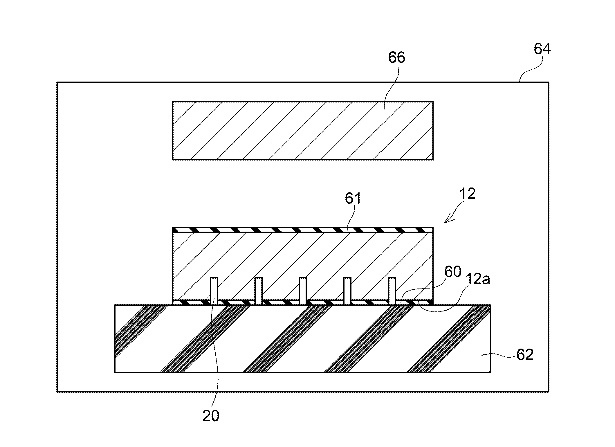
The patent describes a method for manufacturing a semiconductor device by forming a trench in a surface of a SiC substrate and covering it with a protective substrate. The protective substrate prevents the sublimation of silicon from the side surface of the trench during annealing. This method ensures the formation of a protective film on the side surface of the trench and suppresses the substrate's sublimation during the annealing process. This ultimately results in a more robust semiconductor device.

Problems solved by technology

In this case, if a protective film is intended to be formed on the front surface of the SiC substrate, before annealing, for the purpose of preventing sublimation of Si, the protective film cannot appropriately be formed on a side surface of the trench.
For example, if the protective film is formed by a plasma CVD method or sputtering, the protective film on the side surface of the trench becomes extremely thin.
Furthermore, if the protective film is formed by a thermal CVD method, the protective film on the side surface of the trench becomes sparse.
Accordingly, it was not possible to suppress sublimation of Si from the side surface of the trench.

Method used


Image

  • Manufacturing method of semiconductor device
  • Manufacturing method of semiconductor device
  • Manufacturing method of semiconductor device

Examples


Embodiment Construction

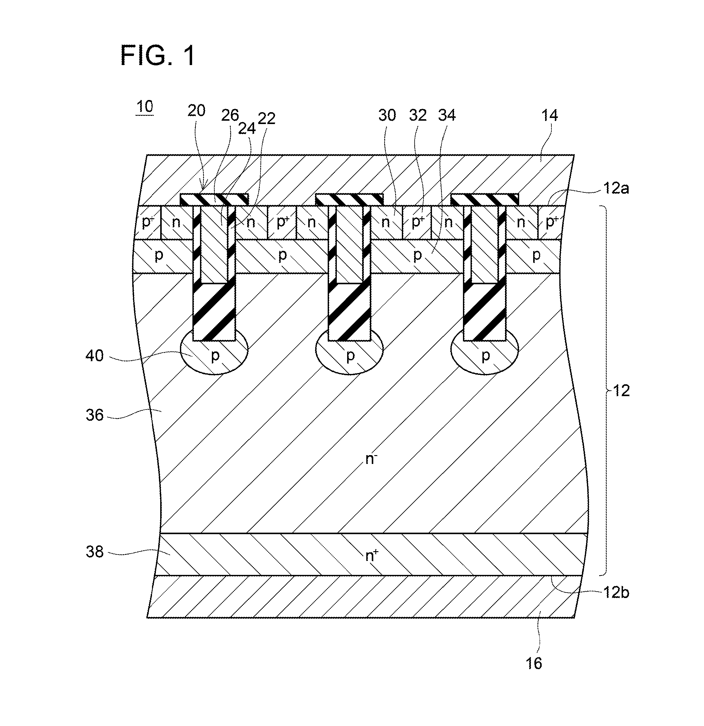
[0018]FIG. 1 shows a MOSFET 10 manufactured by a method according to the present embodiment. The MOSFET 10 has a SiC substrate 12. The SiC substrate 12 consists of SiC (silicon carbide). A source electrode 14 is formed on a front surface 12a of the SiC substrate 12. A drain electrode 16 is formed on a back surface 12b of the SiC substrate 12.

[0019]A trench 20 is formed in the front surface 12a of the SiC substrate 12. An inner surface of the trench 20 is covered with a gate insulation film 22. The gate insulation film 22 portion that covers a bottom surface of the trench 20 is thicker than the gate insulation film 22 portion that covers a side surface of the trench 20. A gate electrode 24 is positioned inside each trench 20. The gate electrode 24 is insulated from the SiC substrate 12 by the gate insulation film 22. An upper surface of the gate electrode 24 is covered with an interlayer insulation film 26. The gate electrode 24 is insulated from the source electrode 14 by the interl...


PUM


Abstract

A manufacturing method of a semiconductor device is provided by forming a trench in a surface of a SiC substrate, positioning a protective substrate to cover the trench, and annealing the SiC substrate and the protective substrate.

Description

CROSS-REFERENCE TO RELATED APPLICATION[0001]This application claims priority to Japanese Patent Application No. 2015-041260 filed on Mar. 3, 2015, the entire contents of which are hereby incorporated by reference into the present application.TECHNICAL FIELD[0002]The technology disclosed herein relates to a manufacturing method of a semiconductor device.DESCRIPTION OF RELATED ART[0003]Japanese Patent Application Publication No. 2008-283143 discloses a technology to form a protective film that consists of Carbon on a front surface of a SiC substrate, and afterwards anneals the SiC substrate. According to this method, the protective film can suppress sublimation of Si from the front surface of the SiC substrate during annealing.BRIEF SUMMARY[0004]There may be a case where the SiC substrate, which has had a trench formed in its front surface, thereafter needs annealing. In this case, if a protective film is intended to be formed on the front surface of the SiC substrate, before annealin...

Claims


Application Information

Patent Timeline
IPC IPC(8): H01L21/04H01L21/683H01L21/324
CPCH01L21/0475H01L21/0455H01L2221/6834H01L21/6835H01L21/324H01L29/1608H01L21/046H01L21/02529H01L21/045H01L21/02378
Inventor IKEDA, TOMOHARUMIYAHARA, SHINICHIROAOI, SACHIKO
Owner TOYOTA JIDOSHA KK
Learn More