Organic light emitting diode display device and method of manufacturing the same

a technology of light-emitting diodes and display devices, which is applied in the direction of organic semiconductor devices, solid-state devices, semiconductor devices, etc., can solve the problems of reducing the adhesion between a substrate and an encapsulation structure, and reducing the external infiltration of moisture or oxygen therein. , the effect of reducing the infiltration ra

Active Publication Date: 2016-09-15
SAMSUNG DISPLAY CO LTD
View PDF11 Cites 17 Cited by
  • Summary
  • Abstract
  • Description
  • Claims
  • Application Information

AI Technical Summary

Benefits of technology

[0011]In addition, the adhesiveness between a substrate and an encapsulation structure may be enhanced, and the external infiltration of moisture or oxygen thereinto may be reduced or effectively prevented, by removing such a residual organic layer through use of the organic light emitting diode display device and a method of manufacturing the same.

Problems solved by technology

In organic light emitting diode (OLED) display devices, OLED elements are often deteriorated by the infiltration of oxygen or moisture thereinto.
Meanwhile, prior to forming such an encapsulation structure, there may be a case in which a few residual organic layers are unnecessarily or inadvertently deposited while forming an OLED element, for example, at an outer portion of the OLED element.
Because the deposited portion of the OLED element is an area only requiring an inorganic layer, when an organic layer is present in such an area, the adhesiveness between a substrate and an encapsulation structure may decrease, such that a peeling-off issue is caused, and such that the external infiltration of moisture or oxygen occurs, thereby resulting in a dark spot defect.

Method used


Image

  • Organic light emitting diode display device and method of manufacturing the same
  • Organic light emitting diode display device and method of manufacturing the same
  • Organic light emitting diode display device and method of manufacturing the same

Examples


##ventive example 1

Inventive Example 1

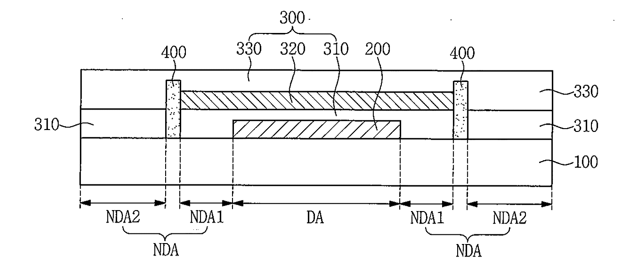
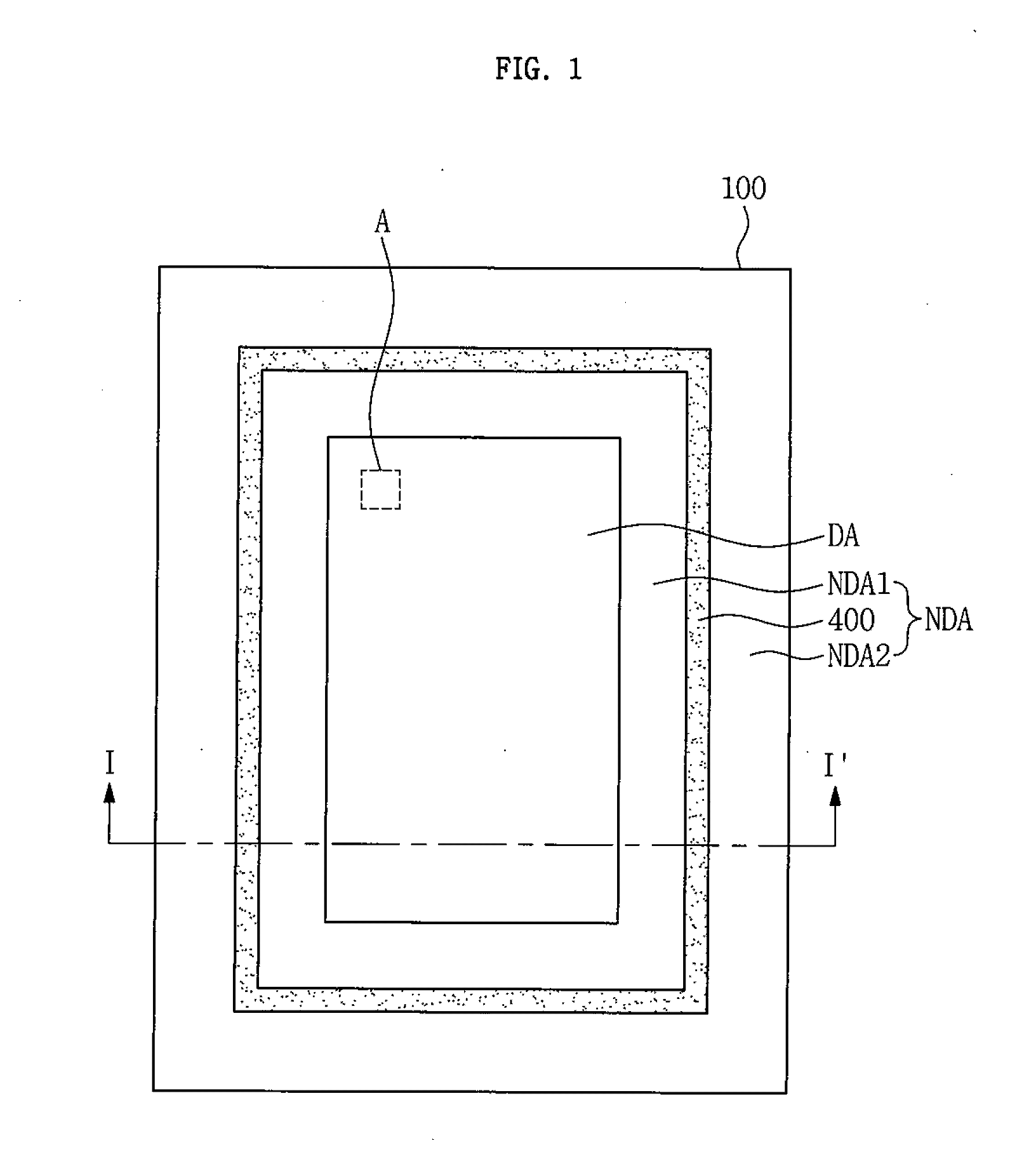
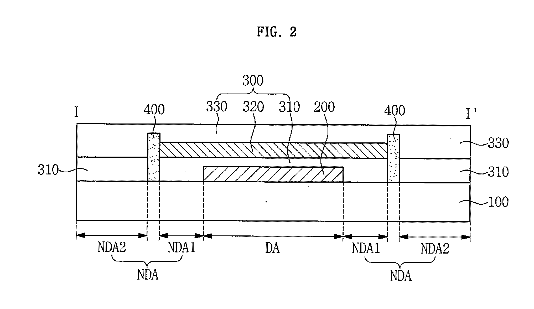
[0140]An OLED element is formed on a substrate, and prior to forming a first inorganic layer of a thin film encapsulation layer, a plasma cleaning treatment is performed. The plasma cleaning treatment is performed on the substrate on which the OLED element is formed, and under a N2 / N2O atmosphere. At the time of performing the plasma cleaning treatment herein, a degree of vacuum (e.g., a degree of pressure) is about 1.5 Torr; a flow rate of N2 gas is about 16,000 standard cubic meters (scm); a flow rate of N2O gas is about 5,000 scm; a level of RF power is 3,000 W; and a period of time for the plasma cleaning treatment is about 10 s.

[0141]The first inorganic layer of the thin film encapsulation layer is formed on the substrate which has undergone the plasma cleaning treatment, and a first organic layer and a second inorganic layer are sequentially deposited on the first inorganic layer, such that the OLED display device is obtained.


PUM

PropertyMeasurementUnit
thicknessaaaaaaaaaa
pressureaaaaaaaaaa
pressureaaaaaaaaaa

Abstract

A method of manufacturing an organic light emitting diode (OLED) display device includes: providing a substrate including a display area and a non-display area; forming an organic light emitting diode element in the display area; forming a barrier wall around the display area and spaced apart from the organic light emitting diode element; performing a plasma treatment on the substrate on which the organic light emitting diode element is formed; and forming a thin film encapsulation layer for coating the organic light emitting diode element, wherein forming the thin film encapsulation layer includes: forming at least one inorganic layer; and forming at least one organic layer inwardly of the barrier wall.

Description

CROSS-REFERENCE TO RELATED APPLICATION[0001]This application claims priority to and the benefit of Korean Patent Application No. 10-2015-0032501, filed on Mar. 9, 2015, with the Korean Intellectual Property Office, the entire content of which is incorporated herein in its entirety by reference.BACKGROUND[0002]1. Field[0003]Aspects of embodiments of the present invention relate to an organic light emitting diode (OLED) display device and a method of manufacturing the same, and more particularly, to an OLED display device enhanced in regard to the adhesiveness between a substrate and an encapsulation structure, and a method of manufacturing the same.[0004]2. Description of the Related Art[0005]In organic light emitting diode (OLED) display devices, OLED elements are often deteriorated by the infiltration of oxygen or moisture thereinto. Accordingly, to reduce or effectively prevent the infiltration of oxygen or moisture, an encapsulation structure for encapsulating and protecting an O...

Claims


Application Information

Patent Timeline
Patent Type & Authority Applications(United States)
IPC IPC(8): H01L51/52H01L27/32H01L51/00H01L51/56
CPCH01L51/5256H01L51/56H01L2227/323H01L51/004H01L2251/301H01L27/3246H10K59/122H10K50/8445H10K71/00H10K50/841
Inventor KIM, MIKYUNGLEE, SUNYOUL
Owner SAMSUNG DISPLAY CO LTD
Why Eureka
Try Eureka