Fingerprint information detection circuit

Active Publication Date: 2016-09-22
SILEAD
View PDF0 Cites 8 Cited by
  • Summary
  • Abstract
  • Description
  • Claims
  • Application Information

AI Technical Summary

Benefits of technology

[0040]Thus, the distances from the first capacitor and the fingerprint to the feedback unit are non-linear. Hence, the second voltage signal generated by the feedback unit due to detection of fingerprint information can accurately represent

Problems solved by technology

It is uniquely special, yet in the personal consumer market, application of fingerprints is not very mature because it is affected by production design on the one hand, and restricted by cost factors on the other hand.
The main reason for the disadvantage of the optical imaging fingerprint identification unit is that it creates a relatively large volume and requires a clean surface; the major restriction for integrated pressure sensing unit is the supper high cost because it is not commonly used; and fingerprint information detection circuit based on

Method used


Image

  • Fingerprint information detection circuit
  • Fingerprint information detection circuit
  • Fingerprint information detection circuit

Examples


Embodiment Construction

[0047]To make the objectives, technical solutions and advantages of the present invention more apparent, detailed descriptions are provided below in conjunction with the drawing for each embodiment of the present invention. However, person having ordinary skill in the art should appreciate that each embodiment of the present invention provides technical details only to facilitate readers to have a better understanding of the present disclosure. Even without such technical details or various alterations and modifications based on the following embodiments, technical solutions within the scope of the present disclosure as provided by the claims can still be realized.

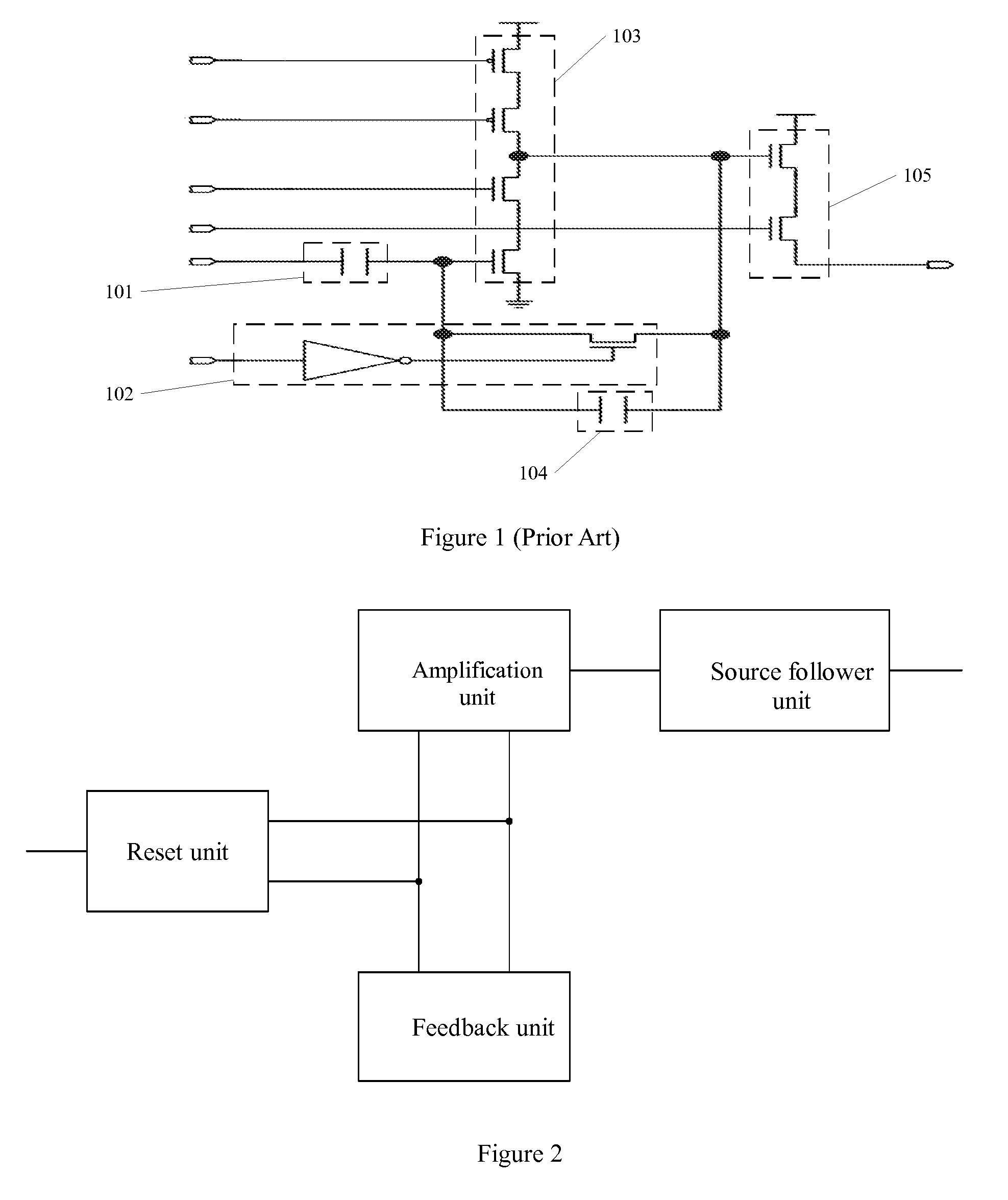
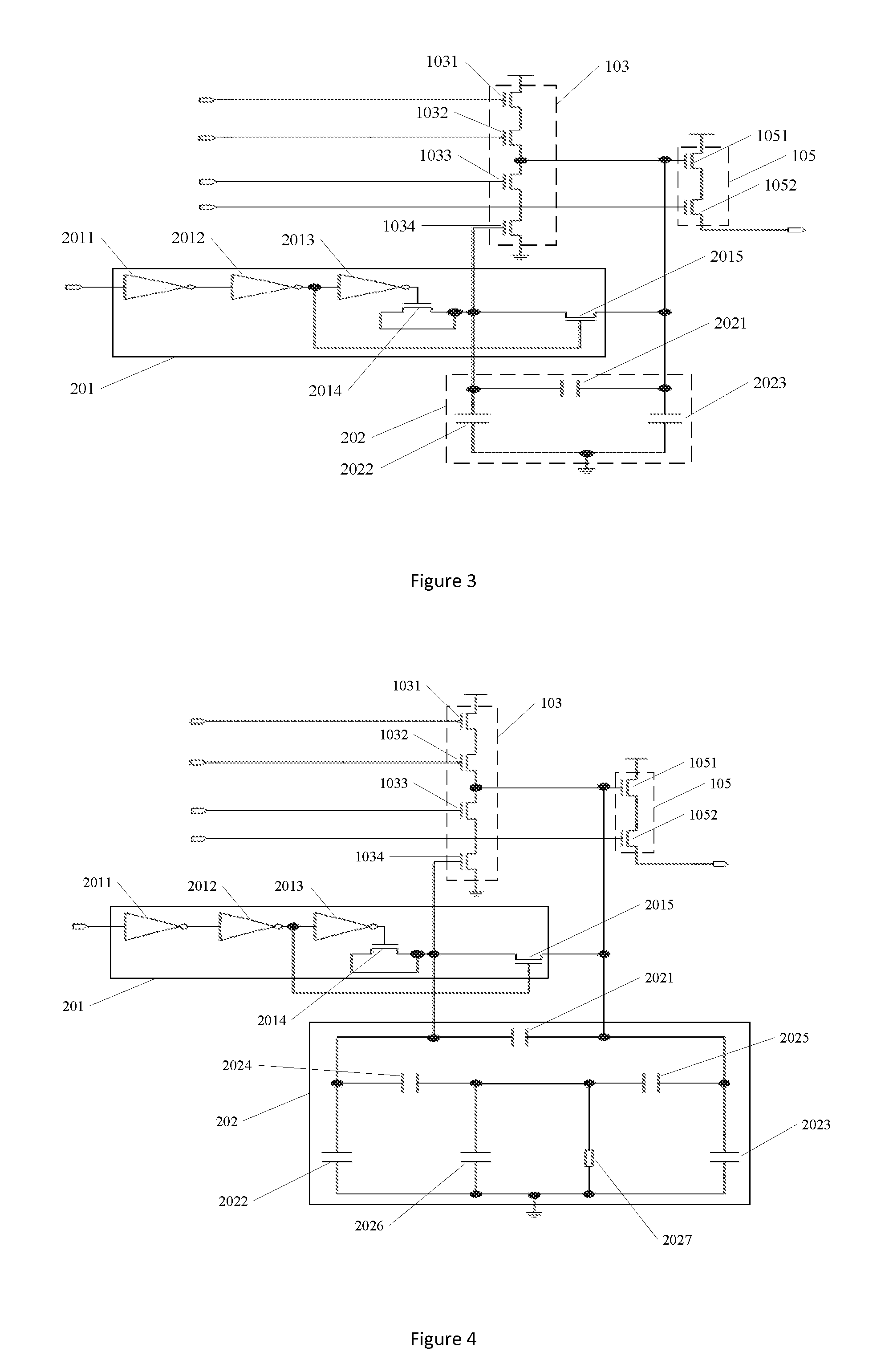
[0048]The first embodiment of the present invention relates to a fingerprint information detection circuit with the specific configuration shown in FIG. 2, which comprises a reset unit, an amplification unit, a feedback unit, and a source follower unit.

[0049]The feedback unit outputs the second voltage signal generated upo...


PUM


Abstract

The present invention relates to a chip design and discloses a fingerprint information detection circuit. The invention includes a reset unit, a feedback unit, an amplification unit and a source follower unit; the reset unit is connected to the feedback unit and amplification unit, while the feedback unit is connected to the amplification unit, and the amplification unit is connected to the source follower unit; when the reset transistor built-into the reset unit is on, it stores an electric charge, and resets the feedback unit; when the reset transistor is off, the stored electric charge is injected into the feedback unit and amplification unit; the feedback unit receives the electric charge, and outputs the second voltage signal generated when it detects fingerprints to the source follower unit; the amplification unit amplifies the received signal and outputs it to the source follower unit; the source follower unit receives the signal, performs voltage level shifting before outputting the first voltage signal that carries the detected fingerprint information. The present invention enables the circuit to use a reduced chip area, hence, saving the cost of the chip.

Description

CROSS-REFERENCE TO RELATED APPLICATIONS[0001]This application is a United States national phase application of co-pending Patent Cooperation Treaty Application No. PCT / CN2014 / 076489, filed Apr. 29, 2014, which claims priority to Chinese Application No. CN2014100582765 filed Feb. 20, 2014, the disclosures of which are incorporated herein by reference.TECHNICAL FIELD[0002]The present invention relates to a chip design, particularly to a fingerprint information detection circuit.BACKGROUND[0003]Biometrics that is used to authenticate and identify personal information is usually realized through physical characteristics (e.g., hair, fingerprints, blood, etc.). When choosing physical characteristics, considerations are given to different aspects, such as the cost of production, ease of processing, reliability, comfort, and so on. Fingerprint is the most reliable feature in biometrics. It is uniquely special, yet in the personal consumer market, application of fingerprints is not very mat...

Claims


Application Information

Patent Timeline
IPC IPC(8): G06K9/00H01L27/06G01N27/22H01L27/092
CPCG06K9/0002H01L27/092H01L27/0629H03K19/00392H03K19/00361G11C29/785G01N27/228G06V40/1306H01L27/0922H01L29/1033H03K17/223
Inventor CHENG, TAIYIZHAO, XIANGGUI
Owner SILEAD
Why Eureka
Try Eureka