Organic el display panel, display device using same, and method for producing organic el display panel

a technology of organic el and display panel, which is applied in the direction of electric lighting source, solid-state device, and light source, can solve the problems of prolonging the operating life of the blue organic el element, prolonging the operating life of the display device, etc., and achieves the effect of improving luminous efficiency and productivity, and high precision

Active Publication Date: 2016-10-06
JOLED INC
View PDF7 Cites 34 Cited by
  • Summary
  • Abstract
  • Description
  • Claims
  • Application Information

AI Technical Summary

Benefits of technology

[0010]According to the organic EL display panel relating to the above aspect having the structure described above, blue light, which is emitted from the blue organic light-emitting layer in each red subpixel region, is converted to red light, and blue light, which is emitted from the blue organic light-emitting layer in each green subpixel region, is converted to green light, and then the converted light is emitted as

Problems solved by technology

The blue organic EL elements tend to have the shortest operating life among the respective organic EL elements of the R, G, and B colors, and accordingly the

Method used


Image

  • Organic el display panel, display device using same, and method for producing organic el display panel
  • Organic el display panel, display device using same, and method for producing organic el display panel
  • Organic el display panel, display device using same, and method for producing organic el display panel

Examples


embodiment 1

[0053]In Embodiment 1, explanation is given on an organic EL display panel of the top emission type.

[0054]100>

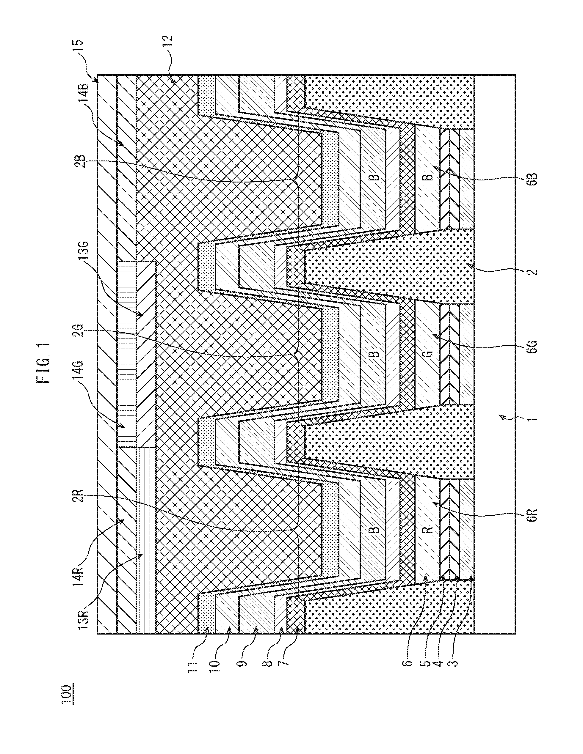
[0055]FIG. 1 is a cross-sectional view schematically showing the pixel structure in the organic EL display panel 100 relating to Embodiment 1. The organic EL display panel 100 (hereinafter, abbreviated as display panel 100) includes pixels that are each composed of red (R), green (G), and blue (B) subpixels and are regularly arranged in a matrix of rows and columns.

[0056]As shown in FIG. 1, the display panel 100 has a substrate as the base thereof. Anodes 3 are disposed on the substrate 1 spaced from each other. A barrier rib 2 (hereinafter, referred to as bank 2) is disposed on the substrate 1, and has openings 2R, 2G, and 2B that are provided therein so as to correspond in position to the red, green, and blue subpixels, respectively.

[0057]Within each opening 2R, a hole injection layer 4, a hole transport layer 5, a red organic light-emitting layer 6R (hereinafter, abbrevia...

embodiment 2

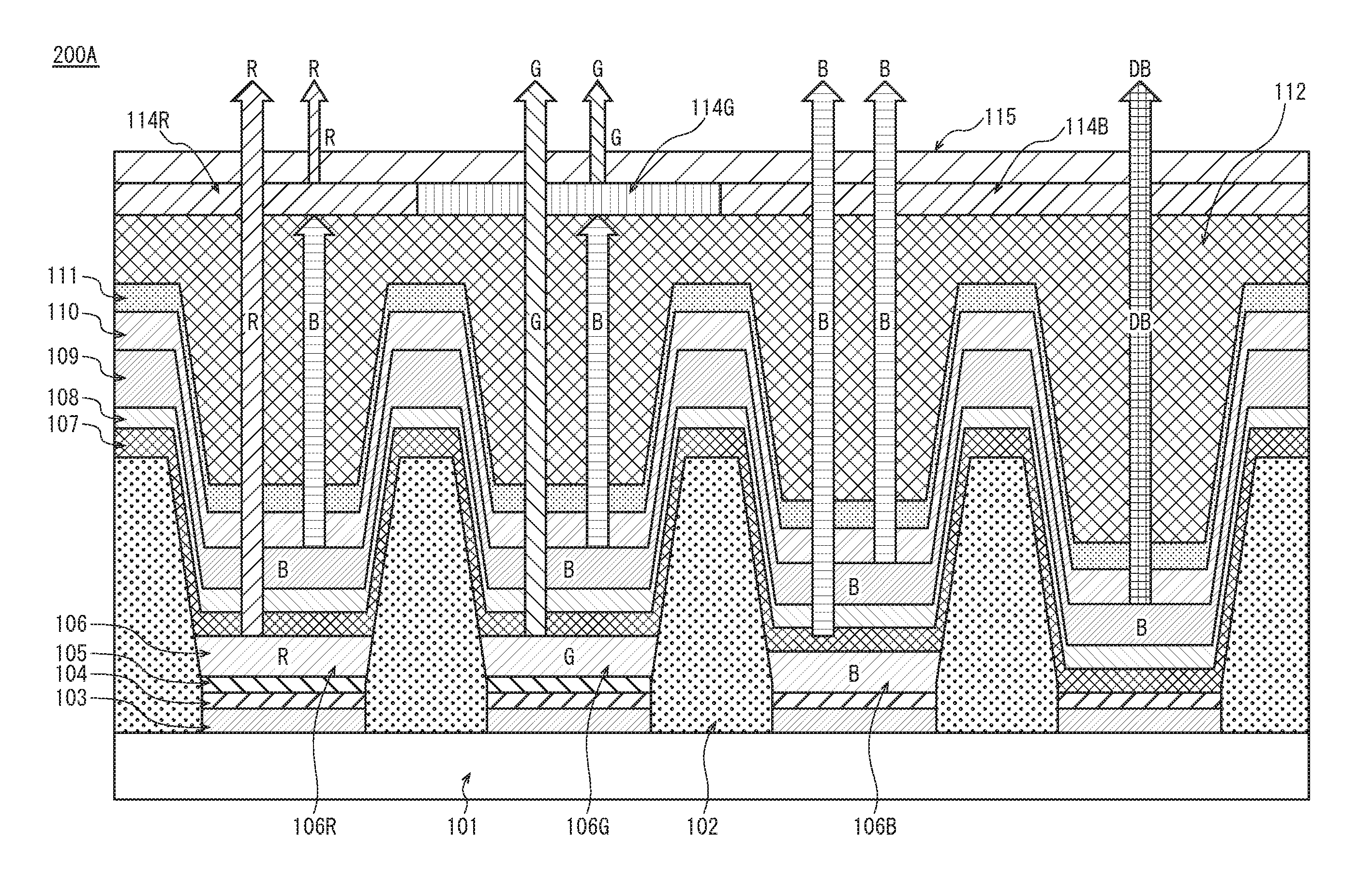
[0174]The following explains an organic EL display panel 200 (hereinafter, abbreviated as display panel 200) relating to Embodiment 2. While the display panel 100 includes pixels each of which is composed of red, green, and blue subpixels, the display panel 200 includes pixels each of which is composed of red, green, and blue subpixels and a subpixel of a dark blue (DB) color emitting dark blue light. This is the difference therebetween. The red, green, and blue subpixels in the display panel 200 are the same as those in the display panel 100, and accordingly explanation thereof is omitted.

[0175]FIG. 11 is a cross-sectional view schematically showing the pixel structure in the display panel 200 relating to Embodiment 2. FIG. 12A to FIG. 14E are views for explaining a manufacturing method of the display panel 200 relating to Embodiment 2.

[0176]In FIG. 11A to FIG. 12G, the display panel 200 has the same structure as the display panel 100 in terms of the materials and the manufacturing...


PUM


Abstract

An organic EL display panel includes: a first pixel electrode and a red organic light-emitting layer sequentially disposed in red subpixel region; a second pixel electrode and a green organic light-emitting layer sequentially disposed in green subpixel region; a third pixel electrode and a first blue organic light-emitting layer sequentially disposed in blue subpixel region; a charge generation layer disposed above the red, green, and first blue light-emitting layers; a second blue organic light-emitting layer disposed on the charge generation layer in the entire subpixel regions; a counter electrode disposed above the second blue light-emitting layer in the entire subpixels regions; a first light conversion layer disposed above the second blue light-emitting layer in the red subpixel region, and converts blue light to red light; and a second light conversion layer disposed above the second blue light-emitting layer in the green subpixel region, and converts blue light to green light.

Description

TECHNICAL FIELD[0001]The present disclosure relates to an organic electro luminescence (EL) display panel that rely on electroluminescence phenomenon of organic materials, a display device using the same, and a manufacturing method of the organic EL display panel.BACKGROUND ART[0002]There have been recently put into practical use, as display panels for display devices such as digital televisions, organic EL panels that include organic light-emitting elements arranged on a substrate in a matrix and rely on electroluminescence phenomenon of organic materials.[0003]A commonly known structure of such organic EL display panels is that drive circuits (for example, including thin film transistor (TFT) elements) are disposed on a substrate, an insulating layer is disposed on the drive circuits, and organic light-emitting elements are further arranged on the insulating layer. The organic light-emitting elements each include, as the basic structure, an anode that is disposed on the insulating...

Claims


Application Information

Patent Timeline
IPC IPC(8): H01L27/32H01L51/56H01L51/00H01L51/50
CPCH01L27/3213H01L27/3211H01L51/504H01L27/322H01L51/5012H01L51/0003H01L51/0008H01L51/0005H01L51/56H05B33/145H10K59/32H10K59/351H10K59/38H10K59/12H10K50/125H10K50/86H10K59/1201H10K50/13H10K59/35H10K71/00H10K71/12H10K71/16H10K71/135H10K50/11G02B5/20
Inventor KOMATSU, TAKAHIRO
Owner JOLED INC
Why Eureka
Try Eureka