Display device and method for driving same

Active Publication Date: 2016-10-13
SHARP KK
View PDF5 Cites 26 Cited by
  • Summary
  • Abstract
  • Description
  • Claims
  • Application Information

AI Technical Summary

Benefits of technology

[0104]According to the first aspect of the present invention, in a display device having pixel circuits, each including an electrooptical element (e.g., an organic EL element) whose luminance is controlled by a current, and a drive transistor for controlling a current to be supplied to the electrooptical element, detection of a characteristic of a circuit element (at least one of the electrooptical element and the drive transistor) is performed during a frame period. Then, a video signal is corrected using correction data which is obtained taking into account a result of the detection. Since a data signal generated based on the thus corrected video signal is supplied to the pixel circuit, a drive current of a magnitude that compensates for degradation of the circuit element is supplied to the electrooptical element. Here, the characteristic of the circuit element is detected by measuring a current flowing through a data signal line. That is, the data signal line is not only used as a signal line that transfers a signal for allowing an electrooptical element in each pixel circuit to emit light at a desired luminance, but also used as a signal line for characteristic detection. Hence, new signal lines do not need to be provided in the display unit to detect characteristics of circuit elements. Accordingly, it becomes possible to compensate for degradation of the circuit elements while an increase in circuit size is suppressed.
[0105]In addition, during an AD conversion period, by a second switch going into an off state, analog data obtained during a monitoring period is held in an output and current-monitoring circuit. Using this function of holding analog data (sample and hold function), an AD conversion circuit is shared between a plurality of columns. This effectively suppresses an increase in circuit size associated with implementation of a configuration capable of detecting characteristics of the circuit elements.
[0106]According to the second aspect of the present invention, detection of characteristics of an electrooptical element and a drive transistor is performed during a frame period. Hence, it becomes possible to compensate for both of degradation of the electrooptical element and degradation of the drive transistor while an increase in circuit size is effectively suppressed.
[0107]According to the third aspect of the present invention, during an AD conversion period included in a drive

Problems solved by technology

As for an organic EL display device employing the passive matrix system, its structure is simple, but a large size and high definition are difficult to achieve.
However, regarding the thin film transistor, variations in threshold voltage tend to occur.
When variations in thresho

Method used


Image

  • Display device and method for driving same
  • Display device and method for driving same
  • Display device and method for driving same

Examples


Example

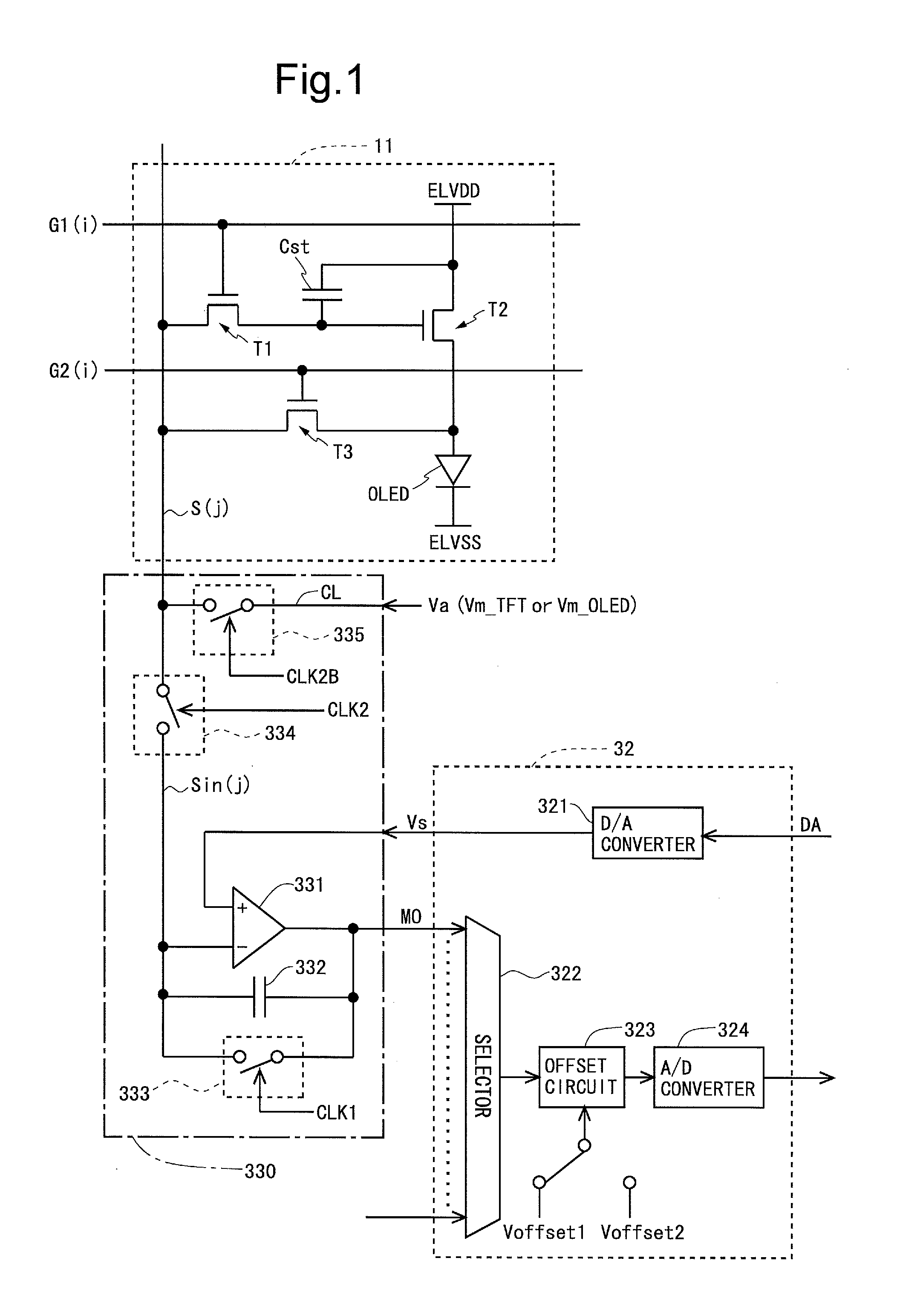
[0154]One embodiment of the present invention will be described below with reference to the accompanying drawings. Note that in the following it is assumed that m and n are integers greater than or equal to 2, i is an integer between 1 and n, inclusive, and j is an integer between 1 and m, inclusive. Note also that in the following a characteristic of a drive transistor provided in a pixel circuit is referred to as “TFT characteristic” and a characteristic of an organic EL element provided in the pixel circuit is referred to as “OLED characteristic”.

[0155]

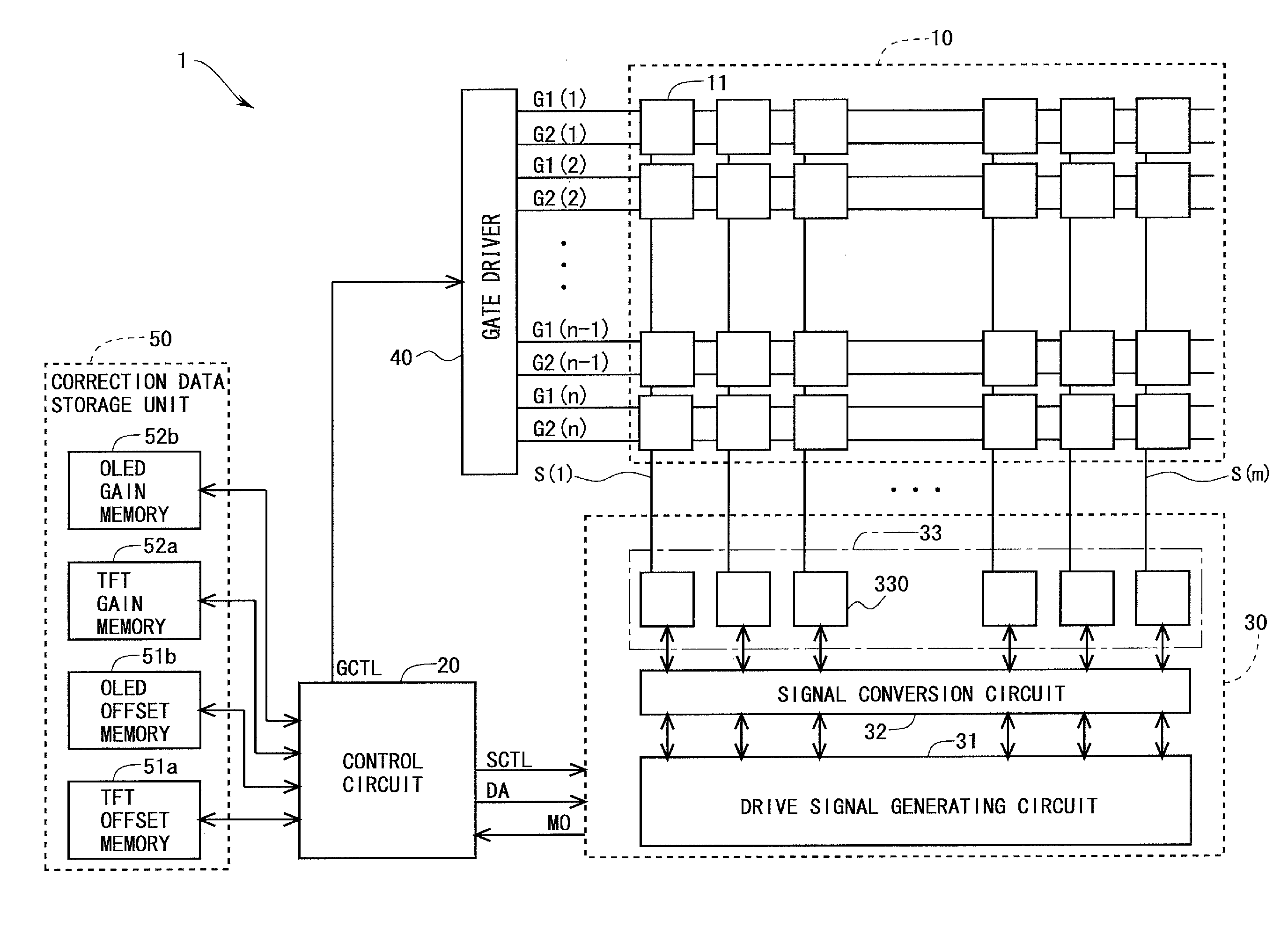
[0156]FIG. 2 is a block diagram showing an overall configuration of an active matrix-type organic EL display device 1 according to one embodiment of the present invention. The organic EL display device 1 includes a display unit 10, a control circuit 20, a source driver (data signal line drive circuit) 30, a gate driver (scanning line drive circuit) 40, and a correction data storage unit 50. In the present embodiment, a pixel circui...


PUM


Abstract

A display device that can compensate for degradation of circuit elements while suppressing an increase in circuit size is implemented.
A data signal line (S(j)) is not only used as a signal line that transfers a signal for allowing an organic EL element (OLED) in each pixel circuit (11) to emit light at a desired luminance, but also used as a signal line for characteristic detection. In addition, a switch (334) is provided between the data signal line (S(j)) and an internal data line (Sin(j)). In such a configuration, during an AD conversion period during which analog data obtained for characteristic detection is converted into digital data, the switch (334) is brought into an off state and a potential of the data signal line (S(j)) obtained immediately before the AD conversion period is supplied from through a predetermined control line (CL) to the data signal line (S(j)).

Description

TECHNICAL FIELD[0001]The present invention relates to a display device and a method for driving the same, and more specifically to a display device provided with a pixel circuit including an electrooptical element such as an organic EL (Electro Luminescence) element, and a method for driving the same.BACKGROUND ART[0002]As a display element provided in a display device, there have hitherto been an electrooptical element whose luminance is controlled by an applied voltage, and an electrooptical element whose luminance is controlled by a flowing current. Examples of the electrooptical element whose luminance is controlled by an applied voltage include a liquid crystal display element. Meanwhile, examples of the electrooptical element whose luminance is controlled by a flowing current include an organic EL element. The organic EL element is also called an OLED (Organic Light-Emitting Diode). An organic EL display device that uses the organic EL element being a spontaneous electrooptica...

Claims


Application Information

Patent Timeline
IPC IPC(8): G09G3/3283G09G3/325
CPCG09G3/3283G09G3/325G09G2330/028G09G2300/0426G09G2320/0295G09G2320/046G09G2300/0819G09G2300/0842G09G2320/0633G09G3/3233G09G2310/0262G09G2320/043G09G2320/045
Inventor KISHI, NORITAKA
Owner SHARP KK
Why Eureka
Try Eureka