Pre-sculpting of si fin elements prior to cladding for transistor channel applications

Active Publication Date: 2016-10-20
TAHOE RES LTD
View PDF0 Cites 19 Cited by
  • Summary
  • Abstract
  • Description
  • Claims
  • Application Information

AI Technical Summary

Problems solved by technology

There are a number of non-trivial issues associa

Method used


Image

  • Pre-sculpting of si fin elements prior to cladding for transistor channel applications
  • Pre-sculpting of si fin elements prior to cladding for transistor channel applications
  • Pre-sculpting of si fin elements prior to cladding for transistor channel applications

Examples


example 15

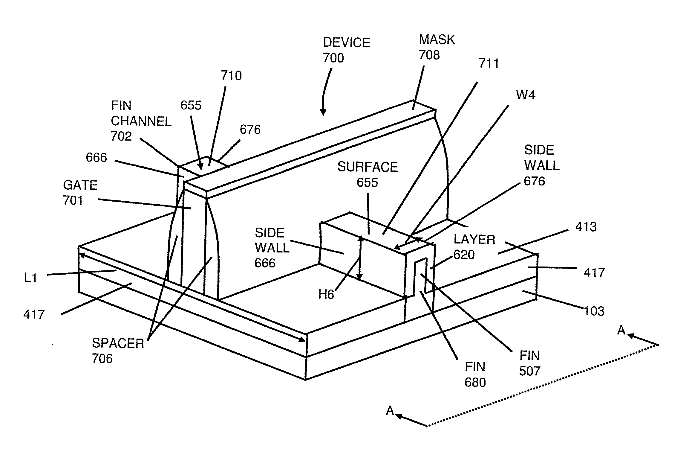
[0115 is an electronic device fin comprising: a narrower upper fin portion formed on and from a wide lower fin portion, the upper and lower portions formed from a substrate of a first single crystal material, the upper and lower portions formed under a first top surface area of the substrate; the wide lower fin portion having wide single crystal top surfaces and wide sidewalls between a first thickness of a trench oxide material in trenches formed between the first top surface areas; and the narrower upper fin portion having narrower single crystal top surfaces and narrower sidewalls with a same single crystal lattice as the wide single crystal top surfaces and the wide sidewalls, wherein the wide single crystal top surfaces and the wide sidewalls have a thickness of between a 1 nm and 15 nm greater than a thickness of the narrower single crystal top surfaces and the narrower sidewalls, the narrower upper fin portion exposed above the first thickness of a trench oxide material in th...


PUM


Abstract

Transistor fin elements (e.g., fin or tri gate) may be modified by radio frequency (RF) plasma and/or thermal processing for purpose of dimensional sculpting. The etched, thinned fins may be formed by first forming wider single crystal fins, and after depositing trench oxide material between the wider fins, etching the wider fins using a second etch to form narrower single crystal fins having undamaged top and sidewalls for epitaxially growing active channel material. The second etch may remove a thickness of between a 1 nm and 15 nm of the top surfaces and the sidewalls of the wider fins. It may remove the thickness using (1) chlorine or fluorine based chemistry using low ion energy plasma processing, or (2) low temperature thermal processing that does not damage fins via energetic ion bombardment, oxidation or by leaving behind etch residue that could disrupt the epitaxial growth quality of the second material.

Description

BACKGROUND[0001]1. Field[0002]Circuit devices and the manufacture and structure of fin based circuit devices.[0003]2. Description of Related Art[0004]Increased performance in and yield of circuit devices on a substrate (e.g., integrated circuit (IC) transistors, resistors, capacitors, etc. on a semiconductor (e.g., silicon) substrate) is typically a major factor considered during design, manufacture, and operation of those devices. For example, during design and manufacture or forming of fin based metal oxide semiconductor (MOS) transistor devices, such as those used in a complementary metal oxide semiconductor (CMOS), it is often desired to increase movement of electrons (carriers) in N-type MOS device (n-MOS) channels and to increase movement of positive charged holes (carriers) in P-type MOS device (p-MOS) channels.[0005]A FinFET may be a transistor built around a thin strip of semiconductor material (generally referred to as the fin). The transistor includes the standard field e...

Claims


Application Information

Patent Timeline
IPC IPC(8): H01L29/66H01L29/04H01L21/306H01L21/304H01L29/78H01L27/105
CPCH01L29/66818H01L29/785H01L29/04H01L21/30604H01L21/304H01L27/105H01L29/1054H01L29/66795H01L29/41791H01L27/0886H01L29/7849
Inventor GLASS, GLENN A.MURTHY, ANAND S.AUBERTINE, DANIEL B.JOSHI, SUBHASH M.
Owner TAHOE RES LTD
Why Eureka
Try Eureka