Parasitic capacitance reduction structure for nanowire transistors and method of manufacturing

a nanowire transistor and capacitance reduction technology, applied in the field of semiconductor devices, semiconductor devices, semiconductor devices, etc., can solve the problems of difficult short-channel control and maintaining device performan

Active Publication Date: 2016-10-27
TOKYO ELECTRON LTD
View PDF1 Cites 28 Cited by
  • Summary
  • Abstract
  • Description
  • Claims
  • Application Information

AI Technical Summary

Benefits of technology

[0006]According to one embodiment, a method is provided for forming a nanowire transistor. The method includes providing a substrate, forming a first nanowire on the substrate, forming a second nanowire on the first nanowire, forming a first dielectric layer between the substrate and the first nanowire, and forming a second dielectric layer between first dielectric layer and the first nanowire, where the second dielectric layer has a higher dielectric constant

Problems solved by technology

However, maintaining the device performance and good short chann

Method used


Image

  • Parasitic capacitance reduction structure for nanowire transistors and method of manufacturing
  • Parasitic capacitance reduction structure for nanowire transistors and method of manufacturing
  • Parasitic capacitance reduction structure for nanowire transistors and method of manufacturing

Examples


Embodiment Construction

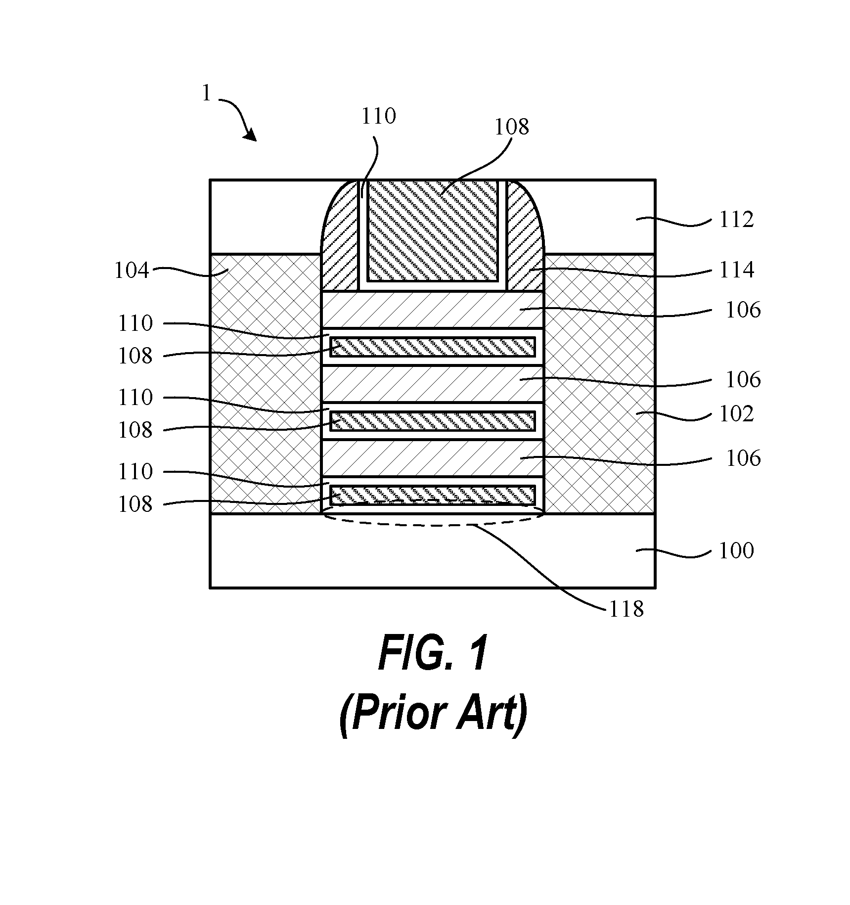
[0014]FIG. 1 schematically shows a cross-sectional view of a prior art nanowire transistor 1 formed on a substrate. The nanowire transistor 1 may be formed using conventional semiconductor manufacturing methods. The nanowire transistor 1 is formed on a substrate 100 and contains source / drains regions 102 / 104, hard mask 112, sidewall spacer 114, nanowires 106, high-k layer 110, and metal gate layer 108. The nanowires 106 may, for example, consist of epitaxial Si or epitaxial SiGe materials.

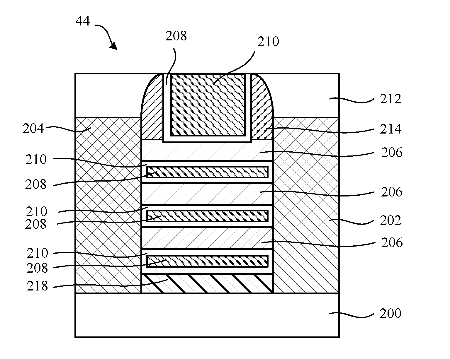
[0015]FIG. 1 further shows a nanowire transistor region 118 that the inventors have identified as having high parasitic capacitance and high current leakage (Toff) when the nanowire transistor 1 is in the OFF state. The nanowire transistor region 118 includes the substrate 100, the high-k layer 110, and the metal gate layer 108. Embodiments of the invention provide a method for reducing the parasitic capacitance and Ioff in the nanowire transistor region 118.

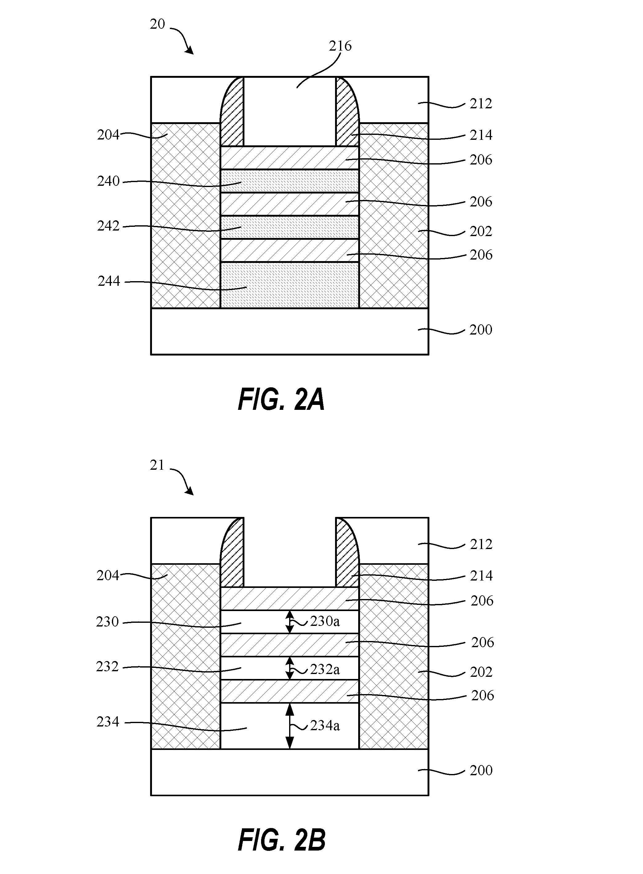
[0016]FIGS. 2A-2H schematically show thr...


PUM


Abstract

Embodiments of the invention describe parasitic capacitance reduction structure for nanowire transistors and method of manufacturing. According to one embodiment the method includes providing a substrate, forming a first nanowire on the substrate, forming a second nanowire on the first nanowire, forming a first dielectric layer between the substrate and the first nanowire, and forming a second dielectric layer between first dielectric layer and the second nanowire, where the second dielectric layer has a higher dielectric constant than the first dielectric layer. According to one embodiment, a nanowire transistor includes a first nanowire on a substrate, a second nanowire on the second nanowire, a first dielectric layer between the substrate and the first nanowire, and a second dielectric layer between the first dielectric layer and the second nanowire, where the second dielectric layer has a higher dielectric constant than the first dielectric layer.

Description

CROSS-REFERENCE TO RELATED APPLICATIONS[0001]This application is related to and claims priority to U.S. Provisional Patent Application Ser. No. 62 / 151,110 filed on Apr. 22, 2015, the entire contents of which are herein incorporated by reference.FIELD OF INVENTION[0002]The present invention relates to the field of semiconductor manufacturing and semiconductor devices, and more particularly to a parasitic capacitance reduction structure for nanowire transistors and method of manufacturing.BACKGROUND OF THE INVENTION[0003]The semiconductor industry has relied on scaling / reducing device feature size in order to boost performance and increase transistor density. The continued device performance improvement due to scaling has seen the introduction of unique technologies such as semiconductor on insulator (e.g., silicon on insulator (SOI) and germanium on insulator (GeOI), stressor such SiGe, SiC to improve mobility at the 90 nm node, epitaxial regrowth of source and drain (raised source a...

Claims


Application Information

Patent Timeline
IPC IPC(8): H01L29/51H01L29/786H01L29/06H01L29/423H01L21/02H01L21/311
CPCH01L29/517H01L21/02532H01L21/02603H01L21/02236H01L29/78696H01L29/0673H01L29/42392H01L29/78654H01L29/78684H01L21/31116H01L29/66439H01L29/775H01L29/1037H01L29/66545H01L29/66742H01L29/66772H01L29/518
Inventor NAKAMURA, GENJITAPILY, KANDABARA N.
Owner TOKYO ELECTRON LTD
Why Eureka
Try Eureka