Semiconductor device and method of manufacturing semiconductor device

a semiconductor and semiconductor technology, applied in the direction of semiconductor devices, basic electric elements, electrical appliances, etc., can solve the problems of lattice defects being leak sources, electrical properties adversely affected, and current leakage,

Active Publication Date: 2016-10-27
FUJI ELECTRIC CO LTD
View PDF0 Cites 4 Cited by
  • Summary
  • Abstract
  • Description
  • Claims
  • Application Information

AI Technical Summary

Benefits of technology

[0015]According to another aspect of the present invention, a method of manufacturing a semiconductor device produces a semiconductor device that includes a semiconductor substrate of a first conductivity type and comprising a semiconductor having a band gap that is wider than that of silicon; a deposited semiconductor layer of the first conductivity type and deposited on a surface of the semiconductor substrate, the first deposited semiconductor layer comprising a semiconductor having a band gap that is wider than that of silicon and an impurity concentration that is lower than that of the semiconductor substrate; a first second-conductivity-type semiconductor region selectively disposed in a surface layer of an opposite side of the first deposited semiconductor layer with respect to a semiconductor substrate side of the first deposited semiconductor layer; an element structure that comprises at least the first second-conductivity-type semiconductor region and a metal layer forming a metal-semiconductor junction on the first deposited semiconductor layer; a second second-conductivity-type semiconductor region that surrounds a periphery of the element structure; and a first conductivity type semiconductor region that surrounds a periphery of the second second-conductivity-type semiconductor region so that the first deposited semiconductor layer is therebetween. The method includes depositing the first deposited semiconductor layer on the surface of the semiconductor substrate; selectively forming as the first conductivity type semiconductor region, a first first-conductivity-type channel stopper region that has an impurity concentration that is higher than that of the first deposited semiconductor layer, the first first-conductivity-type channel stopper region being formed in a surface layer of the first deposited semiconductor layer, at an outer side of a breakdown voltage structure unit that surrounds an active region that bears driving current; and selectively forming as the first conductivity type semiconductor region, a second first-conductivity-type channel stopper region that has an impurity concentration that is at least 10 times that of the first first-conductivity-type channel stopper region, the second first-conductivity-type channel stopper region being formed inside the first first-conductivity-type channel stopper region so as to be encompassed by the first first-conductivity-type channel stopper region.

Problems solved by technology

The depletion layer reaches the chip end where the crystalline structure is in disarray from dicing and causes leak current.
When this high-temperature activation process is executed after the ion implantation of a high impurity concentration is executed, electrical properties are adversely affected consequent to a lattice defect present in the silicon carbide substrate (see, for example, Tsuji, T., et al, “Analyses of high leakage currents in Al+implanted 4H SiC pn diodes caused by threading screw dislocations”, Mater. Sci. Forum Vols.
When a channel stopper whose impurity concentration needs to be a high concentration is formed as a measure against the above, lattice defects are generated to be leak sources.
In this case, the leak is increased when the depletion layer generated due to the interface state reaches the channel stopper.

Method used


Image

  • Semiconductor device and method of manufacturing semiconductor device
  • Semiconductor device and method of manufacturing semiconductor device
  • Semiconductor device and method of manufacturing semiconductor device

Examples


Embodiment Construction

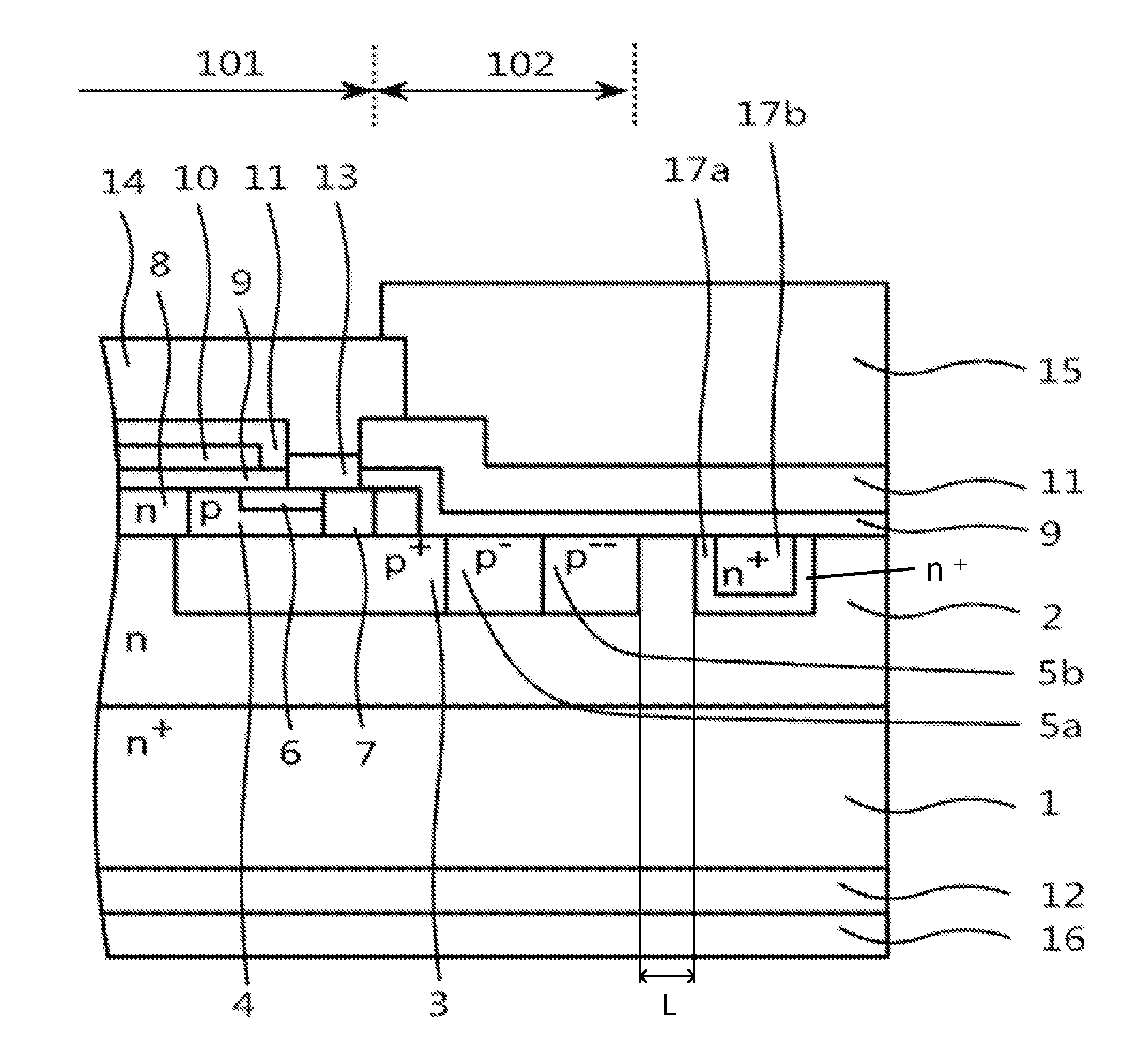
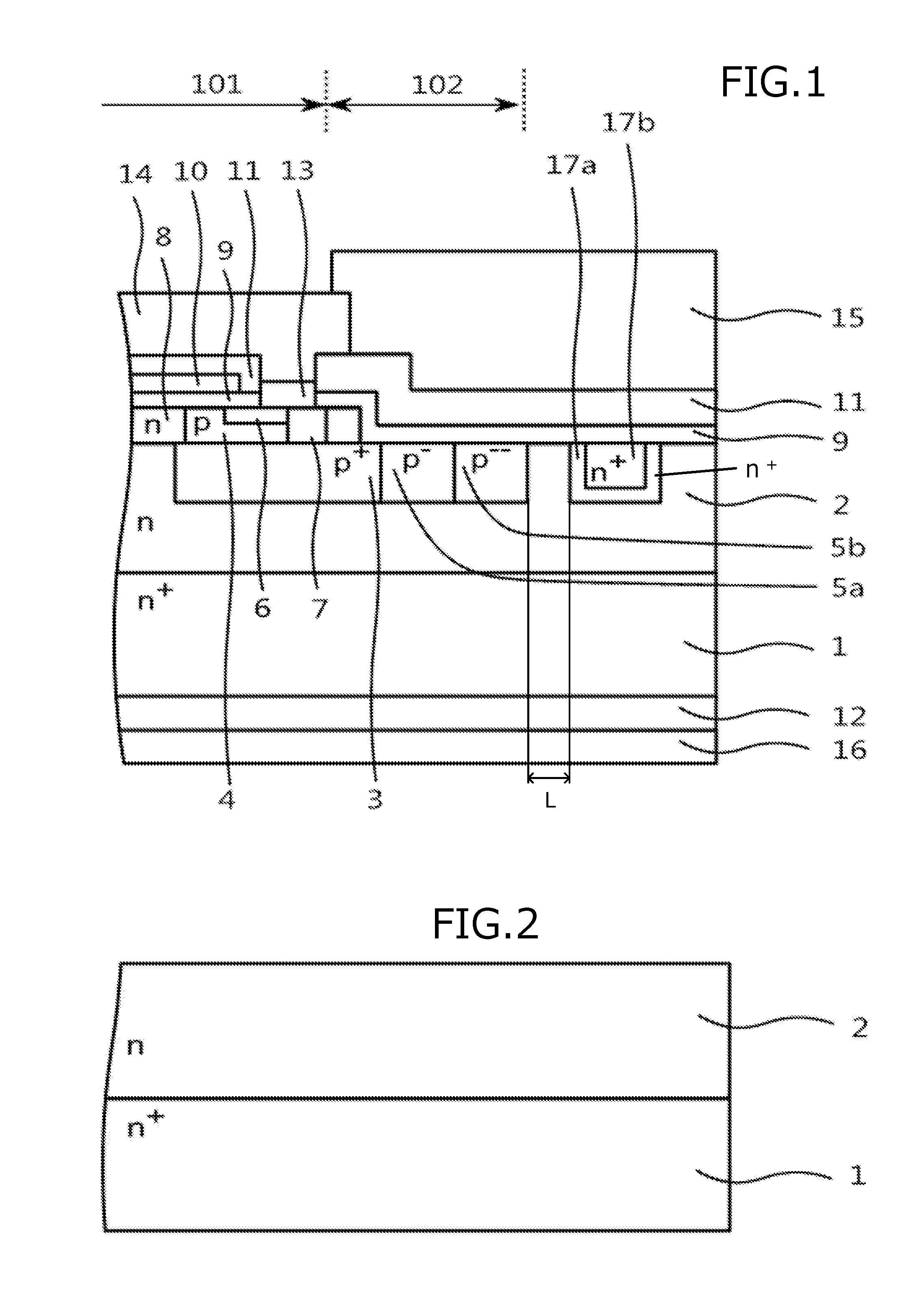
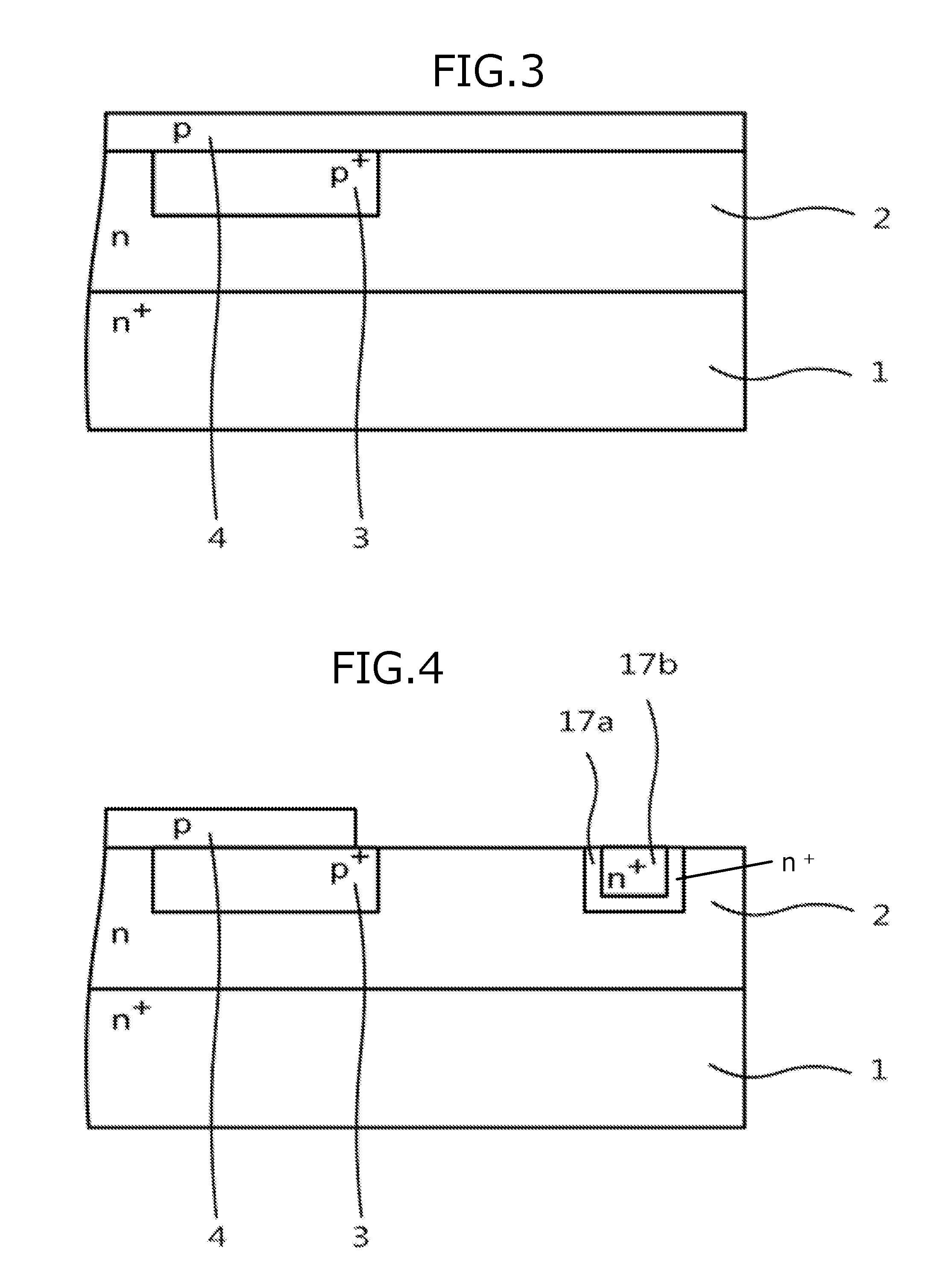
[0022]Preferred embodiments of a semiconductor device and a method of manufacturing a semiconductor device according to the present invention will be described in detail with reference to the accompanying drawings. In the present description and accompanying drawings, layers and regions prefixed with n or p mean that majority carriers are electrons or holes. Additionally, + or − appended to n or p means that the impurity concentration is higher or lower, respectively, than layers and regions without + or −. In the description of the embodiments below and the accompanying drawings, identical constituent elements will be given the same reference numerals and will not repeatedly be described. Further, in the present description, when Miller indices are described, “−” means a bar added to an index immediately after the “−”, and a negative index is expressed by prefixing “−” to the index.

[0023]The semiconductor device according to the present invention is configured using a semiconductor...


PUM

PropertyMeasurementUnit
angleaaaaaaaaaa
off angleaaaaaaaaaa
thicknessaaaaaaaaaa

Abstract

A semiconductor device of an embodiment includes a p+-type region selectively disposed in a surface of an n-type silicon carbide epitaxial layer disposed on an n+-type silicon carbide substrate, an element structure that includes a source electrode and a p+-type region that form a metal-semiconductor junction on the n-type silicon carbide epitaxial layer, a p-type region and another p-type region that surround the periphery of the element structure, and an n+-type channel stopper region that surrounds the periphery of the p-type regions so that the n-type silicon carbide epitaxial layer is therebetween. The n+-type channel stopper region has a second n+-type channel stopper region whose impurity concentration is high, and a first n+-type channel stopper region that encompasses the second n+-type channel stopper region and whose impurity concentration is lower than that of the second n+-type channel stopper region.

Description

CROSS REFERENCE TO RELATED APPLICATIONS[0001]This is a continuation application of International Application PCT / JP2015 / 070337 filed on Jul. 15, 2015 which claims priority from a Japanese Patent Application No. 2014-150257 filed on Jul. 23, 2014, the contents of which are incorporated herein by reference.BACKGROUND OF THE INVENTION[0002]1. Field of the Invention[0003]Embodiments of the invention related to a semiconductor device and method of manufacturing a semiconductor device.[0004]2. Description of the Related Art[0005]Commonly known semiconductor devices use a semiconductor material whose band gap is wider than that of silicon (Si) (hereinafter, “wide band gap semiconductor”) such as silicon carbide (SiC). When a high-voltage device is manufactured using a silicon carbide semiconductor and high voltage is applied, the electric field concentrates at an end of an element. Therefore, a breakdown voltage structure needs to be formed to mitigate the electric field. The surface of th...

Claims


Application Information

Patent Timeline
Patent Type & Authority Applications(United States)
IPC IPC(8): H01L29/78H01L21/761H01L29/06H01L29/66H01L29/04H01L29/16
CPCH01L29/045H01L29/1608H01L29/0638H01L29/7811H01L29/66068H01L21/761H01L29/0623H01L29/0615H01L29/8611
Inventor KINOSHITA, AKIMASAHOSHI, YASUYUKIHARADA, YUICHIOONISHI, YASUHIKO
Owner FUJI ELECTRIC CO LTD
Why Eureka
Try Eureka