Integrated MEMS system

a mems system and integrated technology, applied in the field of integrated mems systems, can solve the problems of growing errors, requiring high sensitivity specifications, and requiring lower bias stability and higher sensitivity specifications

Active Publication Date: 2016-11-03
MOTION ENGINE
View PDF2 Cites 21 Cited by
  • Summary
  • Abstract
  • Description
  • Claims
  • Application Information

AI Technical Summary

Benefits of technology

[0019]In some embodiments, the transducers comprise a six-degree-of-freedom motion sensor, and the parameters comprise three-axes of linear acceleration and three axes of angular rate.
[0020]In some embodiments, the six-degree-of-freedom motion sensor comprises first and second sets of electrodes respectively provided in the first and second cap layers, and a plurality of proof masses provided in the central MEMS layer. The first and second sets of electrodes form capacitors with the proof masses, and some of the first insulated conducting pathways respectively connect the electrodes of the first and second sets of electrodes to at least some of the first cap MEMS-electrical contacts of the first set of MEMS-electrical contacts.

Problems solved by technology

These advanced applications often require lower bias stability and higher sensitivity specifications well beyond the capability of existing consumer-grade MEMS inertial sensors on the market.
Given that MEMS inertial sensors such as accelerometers and gyroscopes are typically much smaller than traditional mechanical gyroscopes, they tend to be subject to higher mechanical noise and drift.
Also, since position and attitude are calculated by integrating the acceleration and angular rate data, respectively, noise and drift lead to growing errors.
These dimensions are approaching the limits of conventional semiconductor processes, particularly photolithographic optical limits.
This mismatch leads to routing difficulties and excessive power consumption, and has led to the introduction of silicon (Si) interposers upon which fine signal distribution traces can be patterned on the chip side and coarse connections patterned on the substrate side with electrical interconnections between the two through the interposer.
The introduction of TSV technology to the IC process adds an additional level of complexity.
Thus, regions of the IC chip must be segregated for TSV fabrication, resulting in inefficient use of the silicon area and higher IC unit cost.
The copper cannot be part of the front-end process because of the temperatures needed to fabricate the IC circuits.
Either approach adds complexity to a semiconductor process that is typically highly controlled and not amenable to modification.
However, there are some fundamental differences between many MEMS fabrication processes and IC fabrication processes.
Additionally, since MEMS transducers are by design sensitive to some environmental influences, MEMS packaging must protect the transducer from undesired environmental influences.
This results in packages that are more complex than those used in standard IC packaging.
The drawback to these approaches is that in general they require additional final packaging including a cap to protect the MEMS and wire bonds to make electrical connection to the IC.
This chip-scale packaging adds considerable expense to the final device.
The cap over the MEMS also makes chip stacking for 3DIC applications difficult, if not impossible.
An integrated motion processing unit has been proposed, however, the costs of individual chip packaging, board fabrication, chip mounting, and mechanical alignment make such approaches costly and useful mainly for high margin applications such as navigation.
Thus, beyond the system components within the chip, no further 3D integration is possible.

Method used


Image

  • Integrated MEMS system
  • Integrated MEMS system
  • Integrated MEMS system

Examples


Embodiment Construction

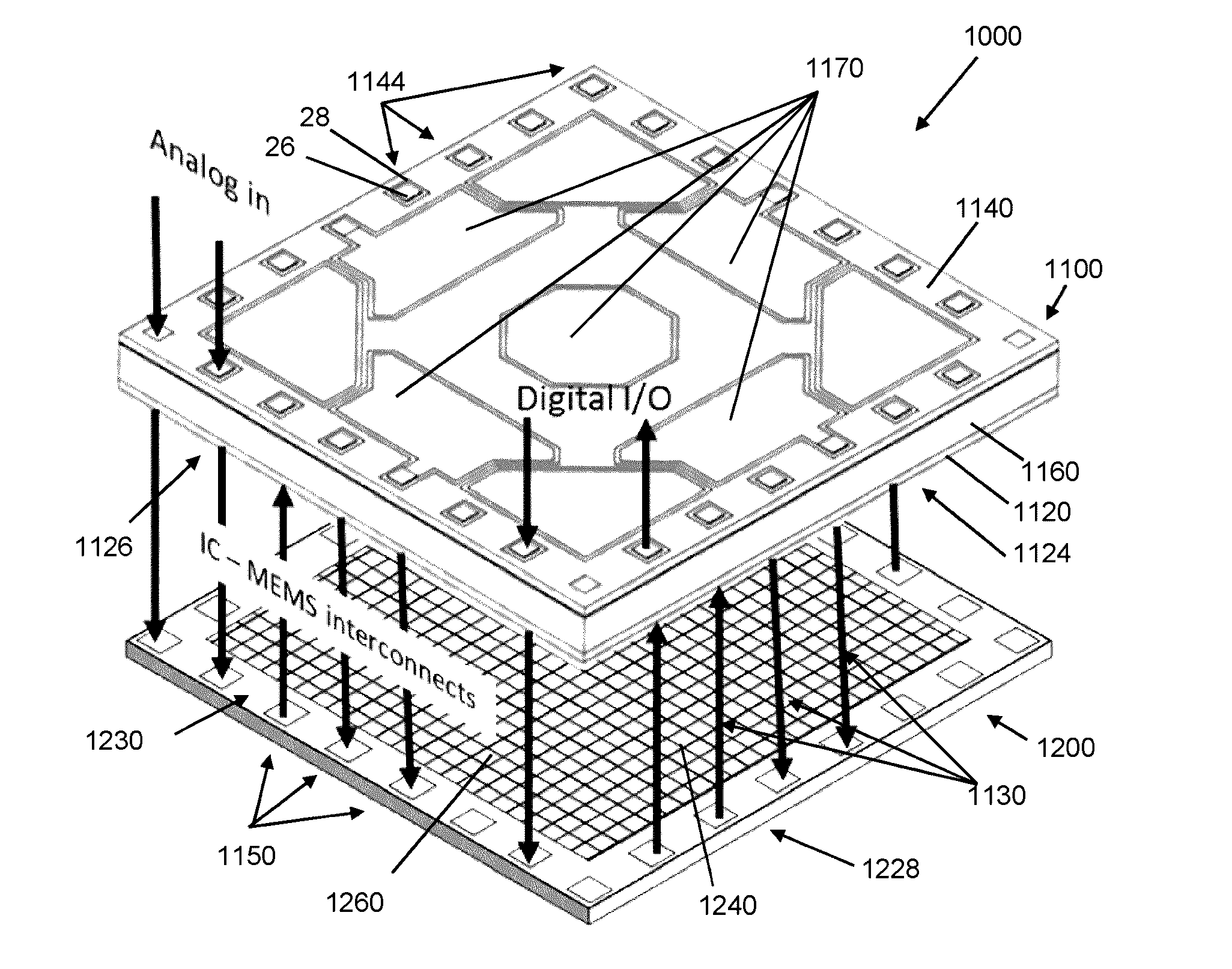
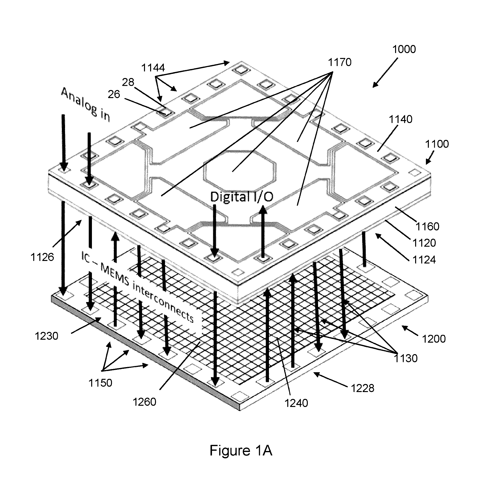
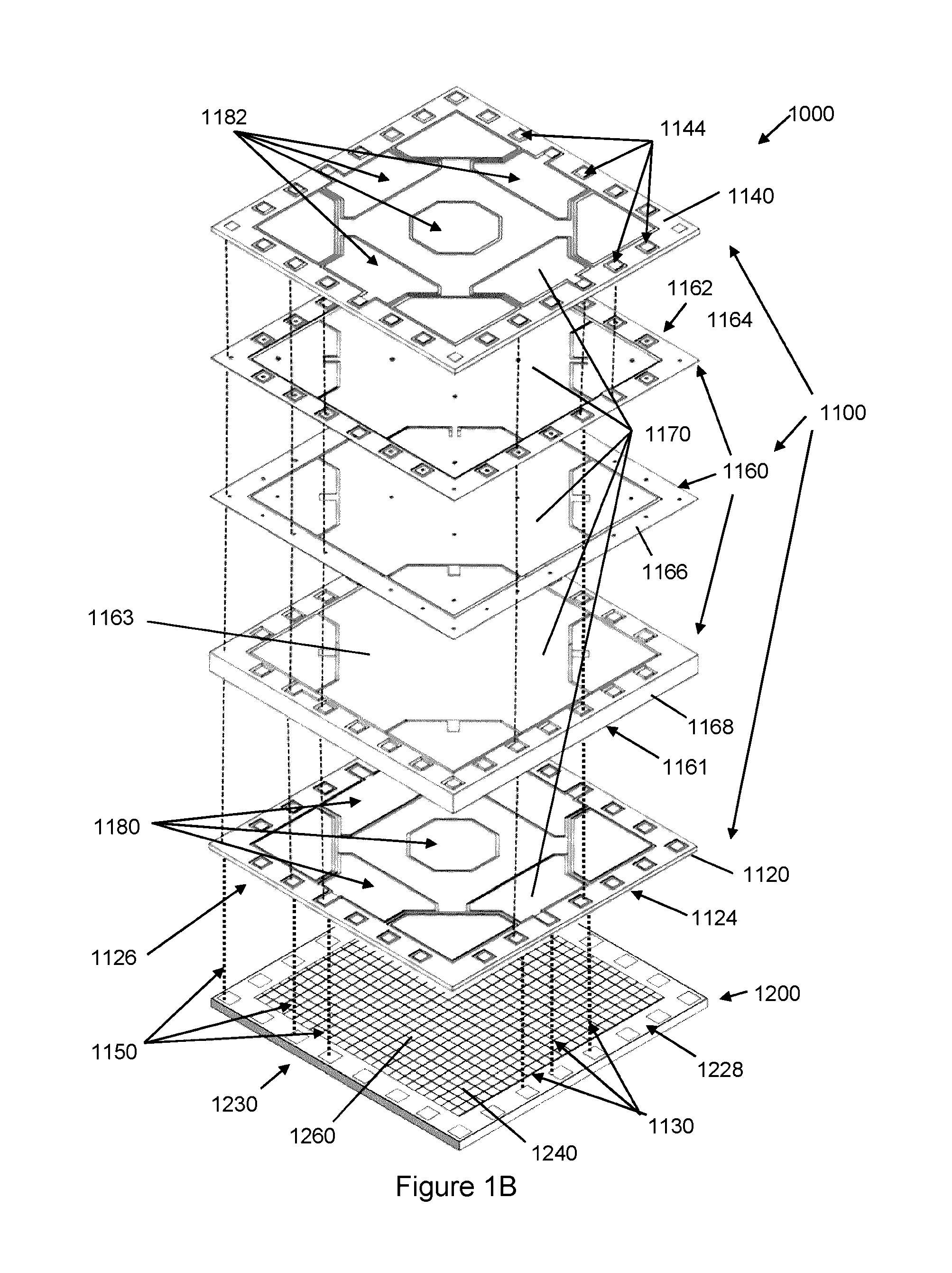
[0038]In the following description, similar features in the drawings have been given similar reference numerals and, in order to preserve clarity in the drawings, some reference numerals may be omitted when they were already identified in a preceding figure. It should also be understood that the elements of the drawings are not necessarily depicted to scale, since emphasis is placed upon clearly illustrating the elements and structures of the present embodiments.

[0039]Throughout the present description, terms such as “top” and “bottom”, “above” and “below”, “over” and “under”, “upper” and “lower”, and other like terms indicating the position of one element with respect to another element are used herein for ease and clarity of description, as illustrated in the figures, and should not be considered limitative. It will be understood that such spatially relative terms are intended to encompass different orientations of the MEMS chips in use or operation, in addition to the orientation...


PUM


Abstract

The present invention provides a 3D System (“3DS”) MEMS architecture that enables the integration of MEMS devices with IC chips to form a System on Chip (SoC) or System in Package (SiP). The integrated MEMS system comprises at least one MEMS chip, including MEMS transducers, and at least one IC chip, including not only MEMS processing circuitry, but also additional/auxiliary circuitry to process auxiliary signals. The MEMS chip can include first and second insulated conducting pathways. The first pathways conduct the MEMS-signals between the transducers and the IC chip, for processing; and the second conducting pathways can extend through the entire thickness of the MEMS chip, to conduct auxiliary signals, such as power, RF, I/Os, to the IC chip, to be processed the additional circuitry.

Description

CROSS-REFERENCE TO RELATED APPLICATIONS[0001]This application is a continuation-in-part of International Application PCT / CA2014 / 051245 filed Dec. 22, 2014, which claims priority to U.S. Provisional Application No. 61 / 925,379 filed Jan. 9, 2014, the entire contents of the above applications being incorporated herein by reference.BACKGROUND OF THE INVENTION[0002]This invention relates to the integration of microelectromechanical systems (MEMS) devices, such as sensors and actuators, and more particularly to an integrated MEMS system including integrated circuits (IC) and MEMS chips.[0003]Micro-electro-mechanical system (MEMS) devices, in particular inertial sensors such as accelerometers and angular rate sensors or gyroscopes, are being used in a steadily growing number of applications. Due to the significant increase in consumer electronics applications for MEMS sensors such as optical image stabilization (OIS) for cameras embedded in smart phones and tablet PCs, virtual reality syst...

Claims


Application Information

Patent Timeline
Patent Type & Authority Applications(United States)
IPC IPC(8): G01P15/18G01P15/125B81B7/00
CPCG01P15/18B81B7/007G01P15/125B81B2207/012B81B2207/07B81B2201/0292B81B2201/0242B81B2201/0264B81B2201/0257B81B2201/0278B81B2201/0235H01L2224/16145G01P15/0802B81C1/00238
Inventor BOYSEL, ROBERT MARKROSS, LOUIS
Owner MOTION ENGINE
Why Eureka
Try Eureka