Touch recognition enabled display device with asymmetric black matrix pattern

a display device and touch recognition technology, applied in the field of display devices, can solve the problems of visual defects, affecting the appearance adding to the thickness and weight of the display device, etc., and achieves the effect of reducing the thickness of the passivation layer, reducing the distance between the electrodes, and reducing the size of the inactive area at the side of the panel

Active Publication Date: 2016-11-03
LG DISPLAY CO LTD
View PDF2 Cites 31 Cited by
  • Summary
  • Abstract
  • Description
  • Claims
  • Application Information

AI Technical Summary

Benefits of technology

[0030]In the embodiments disclosed in the present disclosure, the common signal lines CS_LNs are arranged under the array of TFTs and routed underneath the data lines or the gate lines. Since the common signal lines CS_LNs are routed directly across the active area towards the inactive area, the size of the inactive area at the side of the panel can be reduced. Such configuration also allows reducing the distance between the electrodes that configures the storage capacitor of the pixels. In case of LCD displays, placing the common signal lines CS_LNs away from the layers of the common electrode and the pixel electrode allows to reduce the thickness of the passivation layer between them. Since, the common signal lines CS_LNs can be spaced farther away from the common electrode blocks, they can be provided with a desired thickness to decrease RC delays during touch-sensing period. In addition, undesired fringe field between the pixel electrode PXL and the common signal lines CS_LNs can be kept to minimal when the common electrode blocks arranged in the layer between them. This effectively solves the light leakage problem caused by having the common signal lines CS_LNs in the same layer as the pixel electrode PXL.
[0031]In addition, the masking layer BM is provided with asymmetrically configured masking strips configured to compensate the aperture ratio discrepancy between the pixels caused by the bypass line BP_LN for connecting the common signal lines CS_LNs to the transparent electrode. Within each masking strip, narrower segments (i.e., portions) are provided next to the pixels with reduced aperture ratio due to the bypass lines BP_LNs than the segments positioned between the pixels with the full aperture ratio (i.e., pixels in which the aperture ratio is not directly reduced by the bypass line BP_LN). In this way, the aperture ratio of the bypass pixels (i.e., pixels in which the aperture ratio is reduced by the bypass line BP_LN) is increased while the aperture ratio of the normal pixels is reduced down. Also, the segments, which are positioned next to the bypass pixels with the contact holes for connecting the bypass lines BP_LNs to the corresponding common signal lines CS_LNs and the transparent electrodes, can be shifted in the direction away from the pixels with the contact hole to maximize the aperture ratio of those pixels with the contact hole. Accordingly, the difference in the aperture ratio between the bypass pixels and the normal pixels can be reduced to minimize any visual defects such as moirés.

Problems solved by technology

However, placing a separate substrate for sensing touch inputs on the display panel adds to the thickness and the weight of the display device.
Integrating the touch sensor components within the display panel, however, often necessitates some compromises to be made in the display qualities.
For instance, conductive lines transmitting signals to and from the display regions in the display panel for an implementation of touch-sensing mechanism may generate unwanted parasitic capacitance with other components of the display panel, which may lead to visual defects (e.g., irregular tilting angle of LCD molecules, line dim, etc.).
When implementing a touch sensor within a display panel, fine-tuning of the touch-sensing functionality and the display functionality can be challenging.
Among various types of LCD display panels, arrangement of the components for both functionalities can be especially challenging for the in-plane-switching (IPS) type and the fringe-field-switching (FFS) type LCD display panels as the electrodes for generating fields that controls the orientation of the liquid crystal molecules are provided on the same side of the liquid crystal layer.

Method used


Image

  • Touch recognition enabled display device with asymmetric black matrix pattern
  • Touch recognition enabled display device with asymmetric black matrix pattern
  • Touch recognition enabled display device with asymmetric black matrix pattern

Examples


Embodiment Construction

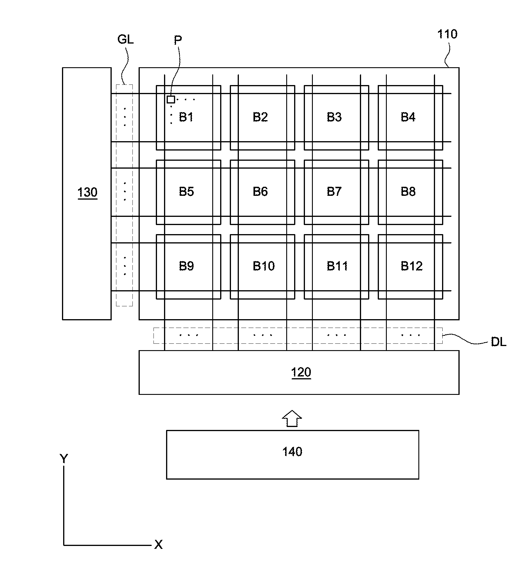
[0044]Reference will now be made in detail to the exemplary embodiments of the present invention, examples of which are illustrated in the accompanying drawings. Wherever possible, the same reference numbers will be used throughout the drawings to refer to the same or like parts.

[0045]The following description includes embodiments described in the context of LCDs, in particular the In-Plane-Switching (IPS) mode LCD and the Fringe-Field-Switching (FFS) mode LCD, in which the common electrodes and the pixel electrodes of the pixels are arranged on one of the substrates that enclose the liquid crystal layer. However, it should be appreciated that the features described here can be used applied to any types of displays having a plurality of conductive lines placed under the array of TFTs, which are connected to the ones of the electrodes shared among a group of pixels. For instance, an organic-light-emitting-diode (OLED) display can be provided with the common signal lines CS_LNs placed...


PUM


Abstract

A touch recognition enabled display device includes a plurality of common electrode blocks serving as touch-sensing regions and/or touch-driving regions. Conductive lines connected to the common electrode blocks are placed under the common electrode blocks and the pixel electrodes of the pixels, and they are routed across the active area, directly toward an inactive area where drive-integrated circuits are located. The conductive lines are positioned under one or more planarization layers, and are connected to the corresponding common electrode blocks via one or more contact holes.

Description

BACKGROUND OF THE INVENTION[0001]1. Field of the Invention[0002]The present disclosure generally relates to a display device, and more particularly to a display device configured for advanced capacitance touch-sensing and a method for manufacturing the same.[0003]2. Description of the Related Art[0004]With ease of use and versatility in operation, touch sensor has been one of the most popular user interaction mechanisms in a variety of electronic devices. In particular, a touch screen allows a user to interact with a device simply by touching the graphical interface displayed on the screen with fingers, stylus or other objects. Thus, the touch screen is applied in various kinds of flat panel displays such as liquid crystal displays (LCDs) and organic light emitting diode (OLED) displays.[0005]Conventionally, a substrate provided with a matrix of touch-driving lines and touch-sensing lines is overlaid across a display panel to provide the touch-sensing functionality. However, placing...

Claims


Application Information

Patent Timeline
Patent Type & Authority Applications(United States)
IPC IPC(8): G06F3/047G06F3/044G09G5/18G09G5/00
CPCG06F3/047G09G5/003G09G2300/0426G09G5/18G06F3/044G06F3/0412G09G3/20G09G2300/023G09G2354/00G06F3/0443G06F3/04184G02F1/13338G02F1/136286G06F3/0446G06F2203/04103G06F3/0416
Inventor KIM, MINGYEONGKIM, TAESANGKIM, SEONGSU
Owner LG DISPLAY CO LTD
Why Eureka
Try Eureka