Printed Circuit Board

a printed circuit board and circuit board technology, applied in the direction of pulse technique, high frequency circuit adaptation, instruments, etc., can solve the problems of affecting the degree of protection, and affecting the degree of integration of such components

Inactive Publication Date: 2016-11-10
AT & S AUSTRIA TECH & SYSTTECHN AG
View PDF7 Cites 7 Cited by
  • Summary
  • Abstract
  • Description
  • Claims
  • Application Information

AI Technical Summary

Benefits of technology

[0008]In order to further increase the degree of integration of such components into a printed circuit board the invention is thus directed to a connection system for electronic components forming components such as microphones and loudspeakers, trackpads and the like within the thickness of the connection system for electronic components. In addition to the favorably small dimensions required on the connection system for electronic components to provide these functionalities, the invention provides improved protection to the components thus formed.
[0010]Since the microphone or the loudspeaker is arranged within the thickness of the printed circuit board and since it is not necessary to provide any openings for the sound to enter the cavity the invention provides for a microphone or a loudspeaker that is sealed against dust and water and is thus not prone to early malfunction.
[0016]Moreover it can be provided that the at least one cavity is at least partly filled with a material adapted to increase the capacitance of the cavity, as it is in accordance with a preferred embodiment of the present invention. In this context it is particularly preferred that the material adapted to increase the capacitance of the cavity is a paste-like material containing barium titanate BaTiO3. Such a material can easily be applied in a cavity in a printed circuit board according to the present invention before applying an electrode-group. BaTiO3 will provide considerably increased capacitance of the capacitor formed in the printed circuit board of the present invention and will thus enable clear signals from the microphone / loudspeaker thus formed.
[0018]In addition to the already described functionalities of microphone and / or loudspeaker the present invention allows for cheap, yet effective production of track pads and other pointing devices and buttons of personal computers, smartphones and the like when the printed circuit board comprises a plurality of cavities to form a plurality of capacitors on the connection system for electronic components as it is in accordance with the preferred embodiment of the present invention. Forming cavities in a printed circuit board is easy to be achieved by techniques well known in the art of the production of printed circuit boards and the present invention thus provides a simple way to arrange a large number of capacitors next to each other in a printed circuit board. When a user touches the printed circuit board or a foil covering the printed circuit board according to the present invention, the capacitor or the capacitors in the proximity of the user's skin change their capacitance and thus yield signals that allow tracking of the user's finger on the track pad or pointing device. This information can be translated into movement of a cursor on a screen as it is well known in computer technology.
[0019]According to a preferred of the present embodiment of the present invention at least one electrode group is glued to the connection system for electronic components. Gluing the electrode-group to the printed circuit board comprising the at least one cavity can be particularly effective when the insulating layers of the electrode groups are made from FaradFlex® dielectric material.
[0020]According to another preferred embodiment of the present invention the at least one electrode-group is fixed to the connection system for electronic components by means of a layer of no-flow-prepreg. Securing insulating layers to a semi-finished printed circuit board by means of a no-flow-prepreg is a technique well known in the art of producing printed circuit boards and can thus easily be carried out to realize the present invention.

Problems solved by technology

In the technical field of printed wiring boards, IC-substrates are known to offer similar functionality in terms of alternately applied conductive and insulating layers, however, IC-substrates are much smaller and often serve to connect a microchip to a printed circuit board.
Especially components such as buttons, trackpads, microphones and loudspeakers consume considerable space on a printed circuit board and there is, thus, the need to provide such functionalities on a printed circuit board without mounting such components on the surface of a printed circuit board.
Failure of the inventive connection system for electronic components will mostly occur as breaking of the electrode groups, be it the insulating layers or the electrodes formed thereon.
Thus, a discontinuous change in the capacitance can be interpreted as failure if the inventive connection system for electronic components.

Method used


Image

  • Printed Circuit Board
  • Printed Circuit Board
  • Printed Circuit Board

Examples


Embodiment Construction

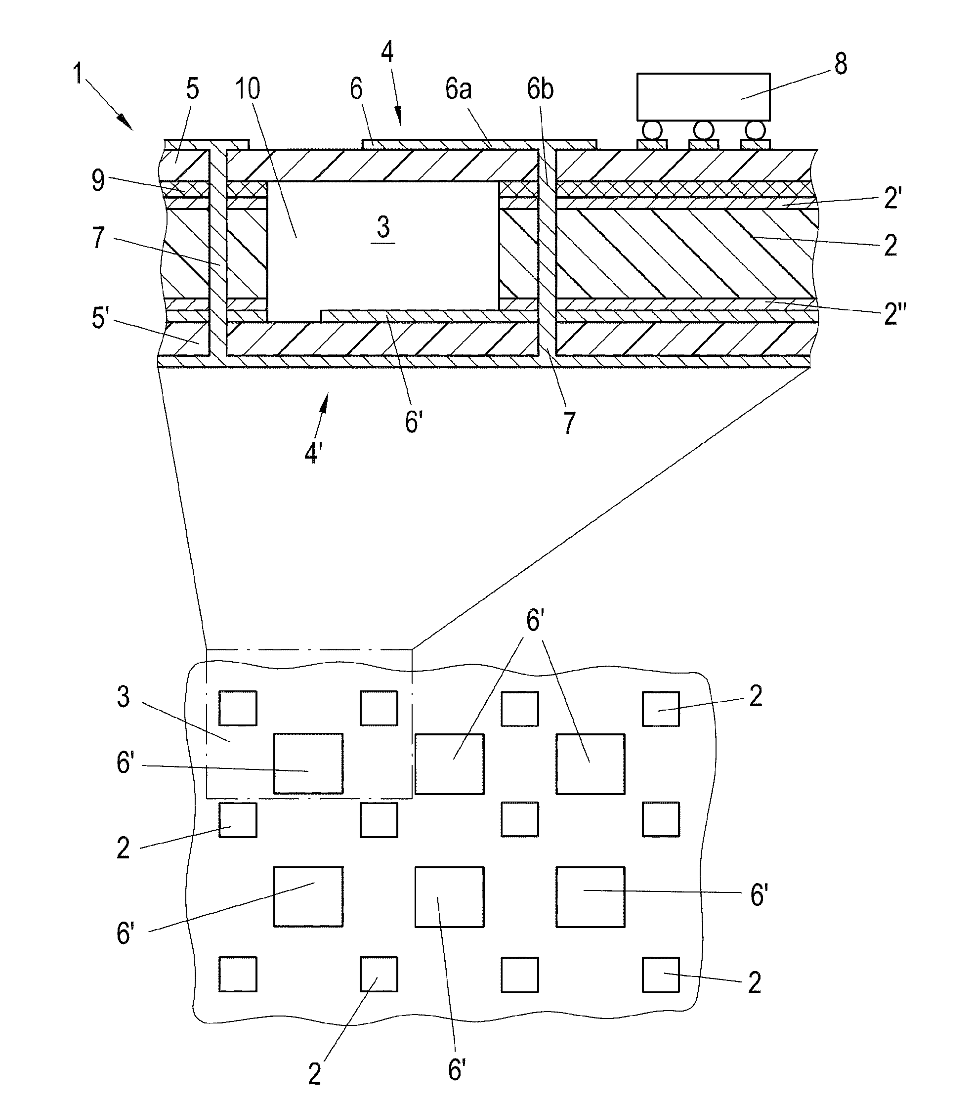
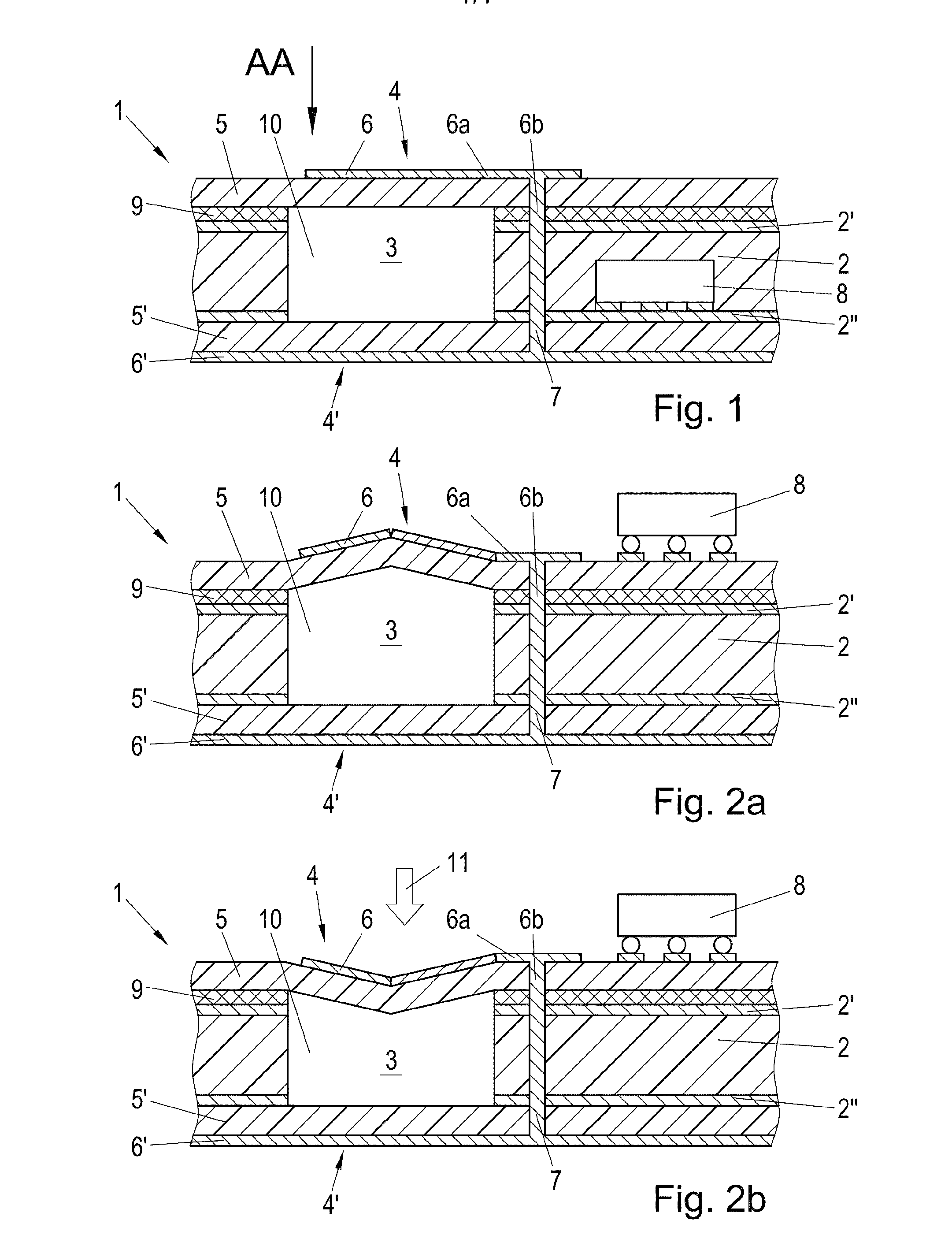
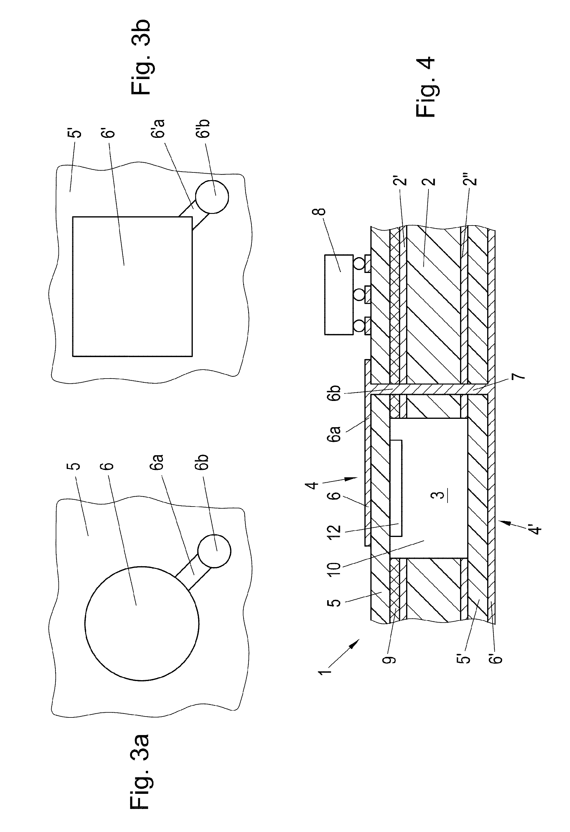
[0037]In FIG. 1 a part of an inventive connection system for electronic components or printed circuit board is denoted by reference numeral 1. The printed circuit board 1 is comprised of a core material of an insulating layer 2 for example formed of prepreg material in which a cavity 3 is formed. The core material, in this case, is a copper-clad laminate having copper layers 2′ and 2″ on either side thereof. The cavity 3 is being covered on both sides thereof by electrode-groups 4 and 4′. The electrode-groups 4, 4′ each are comprised of an insulating layer 5, 5′ followed by a conductive layer 6, 6′. The person skilled in the art will appreciate that the two electrode-groups 4 and 4′ being arranged opposite to each other and being separated by the cavity 3 form electrodes of a capacitor when they are appropriately connected by line 7 to a processing unit 8. In the example according to FIG. 1 the processing unit 8 is embedded within the printed circuit board 1 and it allows for proces...


PUM

PropertyMeasurementUnit
thicknessaaaaaaaaaa
thicknessaaaaaaaaaa
thicknessaaaaaaaaaa

Abstract

In a connection system for electronic components comprising a plurality of insulating layers and conductive layers, and having at least one cavity, the at least one cavity is covered on both sides thereof at least by an electrode-group of an insulating layer followed by a conductive layer, the electrode-groups forming electrodes of a capacitor. A method for detecting failure of a connection system for electronic components comprises the steps of continuously measuring the capacitance of the at least one capacitor formed by the electrode groups and generating a failure message when detecting a discontinuity in the progression of capacitance of the at least one capacitor.

Description

CROSS-REFERENCE TO RELATED APPLICATION[0001]The present invention claims priority to European Application No. 15166936.3, filed May 8, 2015, the disclosure of which is incorporated by reference herein its entirety.BACKGROUND OF THE INVENTION[0002]1. Field of the Invention[0003]The invention relates to a connection system for electronic components comprising a plurality of insulating layers and conductive layers, and comprising at least one cavity, the use of the inventive connection system for electronic components as well as a method for detecting failure of the inventive connection system for electronic components.[0004]2. Description of the Related Art[0005]The invention relates to connection systems for electronic components in general, wherein electronic components such as transistors, integrated circuits (ICs, microchips) and the like are arranged on or embedded within a panel carrying and electrically connecting those electronic components. Such connection systems can be prin...

Claims


Application Information

Patent Timeline
Patent Type & Authority Applications(United States)
IPC IPC(8): H05K1/16H01G5/38H04R19/00G01L9/00G01R27/26H05K1/18H01G5/011
CPCH05K1/162H05K1/181H01G5/38H04R19/005G01L9/0073G01R27/2605H01G5/011H05K1/024H05K1/0293H05K3/4697H05K2201/10083H05K2201/10151H05K2201/10196H03K17/9622H10N30/20
Inventor LEITGEB, MARKUSSTAHR, JOHANNES
Owner AT & S AUSTRIA TECH & SYSTTECHN AG
Why Eureka
Try Eureka