Dye-sensitized solar cell and method for manufacturing thereof

a solar cell and dye sensitization technology, applied in the manufacture of electrolytic capacitors, cell components, cell component details, etc., can solve the problems of high production cost of silicon substrates, unsolved above-mentioned problems, and increase production costs, so as to improve ff, enhance short-circuit current, and high performance

Active Publication Date: 2016-11-24
SHARP KK
View PDF3 Cites 0 Cited by
  • Summary
  • Abstract
  • Description
  • Claims
  • Application Information

AI Technical Summary

Benefits of technology

[0035]According to the present invention, it is possible to provide a high performance dye-sensitized solar cell having an improved FF and an enhanced short-circuit current and a dye-sensitized solar cell module using the cell at low cost.
[0036]In the present invention, since at least two porous semiconductor layers with different light scattering properties are layered in an order of from a layer with lower light scattering property to a layer with higher light scattering property from a light receiving face side of the dye-sensitized solar cell, incident light can efficiently be utilized for photoelectric conversion and a particle diameter of semiconductor particles forming the porous semiconductor layer on an opposite side of the light receiving face is increased. Since the amount of the dye adsorbed in such a porous semiconductor layer is small, the incident light is only absorbed and reflected by the semiconductor particles. In the case where the porous semiconductor layer contains titanium oxide particles, the light absorption region is about 400 nm or shorter and the incident light is absorbed by a carrier transporting material, in which redox seeds such as the titanium oxide particles of the porous semiconductor layer in the light receiving face side and iodine are dissolved, and scarcely reaches the porous semiconductor layer on the opposite side of the light receiving face.
[0037]Accordingly, in the above-mentioned configuration, due to difference of the basic energy levels, no leakage occurs and photoelectric conversion is not dominantly caused in the interface of the photoelectric conversion layer and the catalyst layer, where the leakage is expected to occur, and therefore a porous insulating layer may not be formed. However, in the case of a dye-sensitized solar cell module, the dye-sensitized solar cell of the present invention having no porous insulating layer and a conventional dye-sensitized solar cell having a porous insulating layer may be combined.

Problems solved by technology

However, the former has a problem of a high production cost of the silicon substrates and the latter has a problem that the production cost is increased since various kinds of gases for semiconductor production and complicated production facilities are required.
Therefore, in both solar cells, it has been tried to lower the cost per electric power output by increasing the efficiency of photoelectric conversion; however, the above-mentioned problems still remain while being unsolved.
However, since a basic structure of the dye-sensitized solar cell described in Patent Document 1 is a structure that the electrolytic solution is injected between the opposed transparent conductive film-bearing glass substrates, it is possible to produce a trial solar cell with a small surface area, but it is difficult to practically produce a solar cell with a large surface area such as 1 m square.
As a result, FF (fill-factor) and a short circuit current at the time of the photoelectric conversion are lowered, resulting in a problem of decrease of the photoelectric conversion efficiency.
Further, since the dye-sensitized solar cell module is produced by forming elements between the opposed transparent conductive film-bearing glass substrates, the module has problems that the production cost is increased and the weight is increased.
However, the dye-sensitized solar cell modules described in Patent Document 2 and Non-Patent Document 1 have a configuration that a basic structure of each dye-sensitized solar cell is formed by injecting the electrolytic solution between the opposed transparent conductive film-bearing glass substrates, and therefore the problems of the production cost and weight still remain while being unsolved.
Therefore, the processing steps are increased and the transportation resistance of a carrier transporting material is increased due to the formation of the porous insulating layer, resulting in a problem of deterioration of the performance of the solar cell.
However, if the porous semiconductor layer and the catalyst layer are formed using fine particles, the physical values (energy levels and Schottky barrier between two type materials) of the respective materials cannot often be applied as they are.

Method used


Image

  • Dye-sensitized solar cell and method for manufacturing thereof
  • Dye-sensitized solar cell and method for manufacturing thereof
  • Dye-sensitized solar cell and method for manufacturing thereof

Examples


production example 1

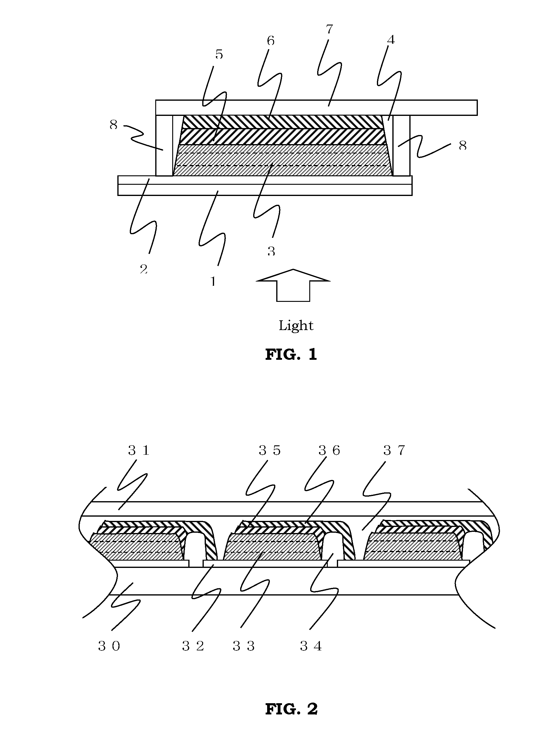
[0172]A solar cell (unit cell) shown in FIG. 1 was produced.

[0173]FIG. 1 is a schematic cross-sectional view of a main part showing the layer structure of a solar cell of the present invention.

[0174]In FIG. 1, a reference numeral 1 denotes a support: a reference numeral 2 denotes a conductive layer: a reference numeral 3 denotes a photoelectric conversion layer filled with a carrier transporting material: a reference numeral 4 denotes a carrier transporting material: a reference numeral 5 denotes a catalyst layer: a reference numeral 6 denotes a counter electrode conductive layer: a reference numeral 7 denotes an output electrode: and a reference numeral 8 denotes a sealing material.

[0175]A glass substrate (trade name: SnO2 film-bearing glass, manufactured by Nippon Sheet Glass Co., Ltd.) obtained by forming a conductive layer 2 of a SnO2 film on a glass support 1 was used. A commercialized titanium oxide paste (trade name: Ti-Nanoxide T / SP, average primary particle diameter of tita...

production example 2

[0187]A solar cell module shown in FIG. 2 was produced.

[0188]FIG. 2 is a schematic cross-sectional view of a main part showing a layer structure of a solar cell module of the present invention. In the drawing, a reference numeral 30 denotes a support: a reference numeral 31 denotes a cover: a reference numeral 32 denotes a conductive layer: a reference numeral 33 denotes a photoelectric conversion layer filled with a carrier transporting material: a reference numeral 34 denotes an inter-cell insulating layer: a reference numeral 35 denotes a catalyst layer: a reference numeral 36 denotes a counter electrode conductive layer: and a reference numeral 37 denotes an insulating layer.

[0189]A glass substrate (trade name: SnO2 film-bearing glass, manufactured by Nippon Sheet Glass Co., Ltd.) obtained by forming a conductive layer 32 of a SnO2 film on a glass support 1 was used. A scribe line was formed in a prescribed site of the conductive layer 32 of the glass substrate by radiating lase...

production example 3

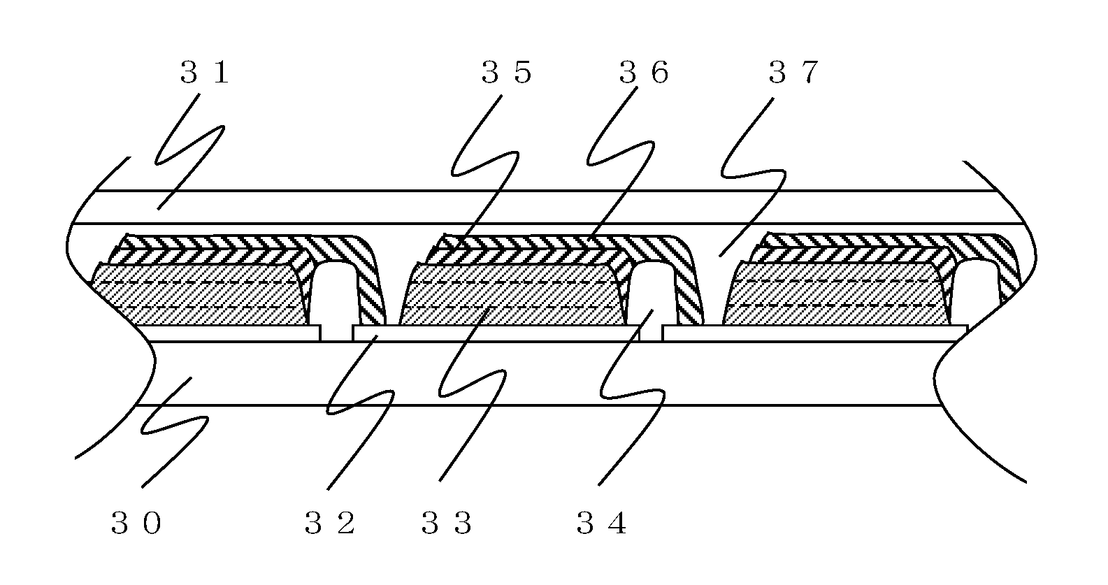
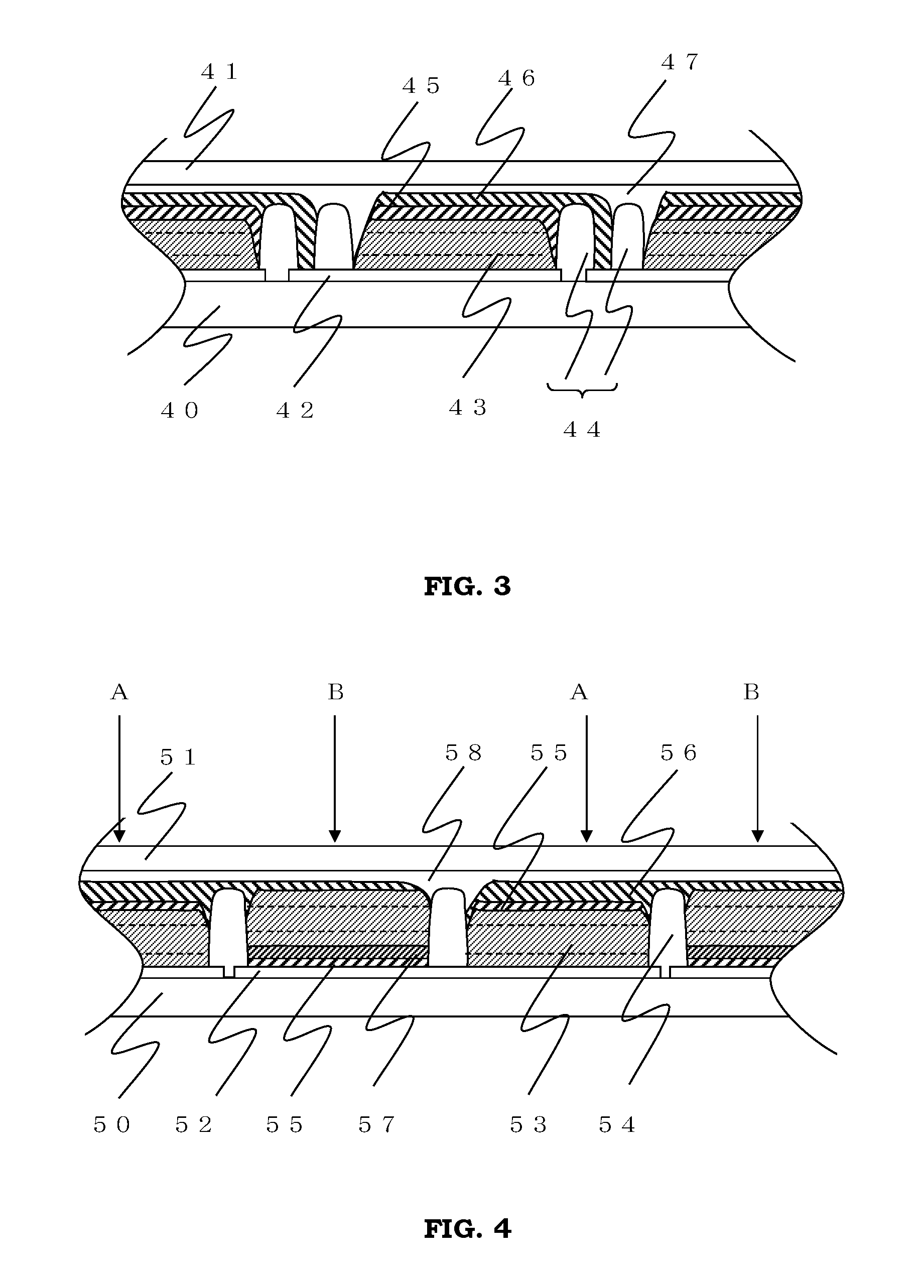
[0193]A solar cell module shown in FIG. 3 was produced.

[0194]FIG. 3 is a schematic cross-sectional view of a main part showing a layer structure of a solar cell module of the present invention. In the drawing, a reference numeral 40 denotes a support: a reference numeral 41 denotes a cover: a reference numeral 42 denotes a conductive layer: a reference numeral 43 denotes a photoelectric conversion layer filled with a carrier transporting material: a reference numeral 44 denotes an inter-cell insulating layer: a reference numeral 45 denotes a catalyst layer: a reference numeral 46 denotes a counter electrode conductive layer: and a reference numeral 47 denotes an insulating layer.

[0195]A solar cell module was completed in the same manner as in Production Example 2, except that after the porous semiconductor layers were formed, two rows of the inter-cell insulating layers 44 were formed an thereafter, the counter electrode conductive layer 46 was formed between the inter-cell insulati...


PUM

PropertyMeasurementUnit
particle diameteraaaaaaaaaa

Abstract

A dye-sensitized solar cell formed by layering a conductive layer; a photoelectric conversion layer in which a dye is adsorbed in a porous semiconductor layer and the layer is filled with a carrier transporting material; and a counter electrode including only a counter electrode conductive layer or including a catalyst layer and a counter electrode conductive layer on a support made of a light transmitting material, in which the photoelectric conversion layer is brought into contact with the counter electrode; the porous semiconductor layer forming the photoelectric conversion layer has two or more layers with different light scattering properties; and the two or more porous semiconductor layers are layered in an order of from a layer with lower light scattering property to a layer with higher light scattering property from a light receiving face side of the dye-sensitized solar cell.

Description

[0001]This application is a continuation of U.S. application Ser. No. 12 / 161,289, filed Jul. 17, 2008, which is the U.S. national phase of International Application No. PCT / JP2006 / 324755, filed Dec. 12, 2006, which designated the U.S. and which claims priority to Japanese Application No. 2006-010132, filed Jan. 18, 2006, the entire contents of each of which are hereby incorporated by reference.TECHNICAL FIELD[0002]The present invention relates to a dye-sensitized solar cell and a dye-sensitized solar cell module.BACKGROUND ART[0003]As an energy source in place of fossil fuel, solar cells capable of converting sun light to electric power have drawn attention. Presently, some of solar cells using crystalline silicon substrates and thin film silicon solar cells have been used practically. However, the former has a problem of a high production cost of the silicon substrates and the latter has a problem that the production cost is increased since various kinds of gases for semiconductor ...

Claims


Application Information

Patent Timeline
Patent Type & Authority Applications(United States)
IPC IPC(8): H01G9/20H01G9/00H01M50/528
CPCH01G9/2063H01G9/2068Y02E10/542H01G9/0029H01G9/2022H01G9/2031
Inventor YAMANAKA, RYOHSUKEFUKE, NOBUHIROFUKUI, ATSUSHI
Owner SHARP KK
Why Eureka
Try Eureka