

Method of manufacturing semiconductor device
a manufacturing method and semiconductor technology, applied in semiconductor devices, semiconductor/solid-state device details, electrical devices, etc., can solve the problems of reducing the function of the barrier metal, reducing the adhesion of the interlayer insulating film and the barrier metal, and unreacted titanium atoms remaining in the titanium nitride film
- Summary
- Abstract
- Description
- Claims
- Application Information
AI Technical Summary
Benefits of technology
Problems solved by technology
Method used
Image

Examples
first embodiment
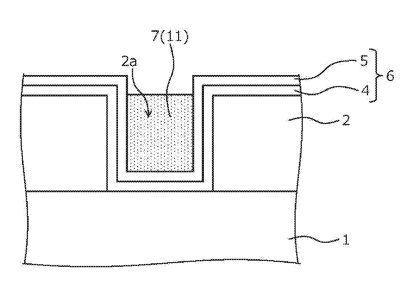
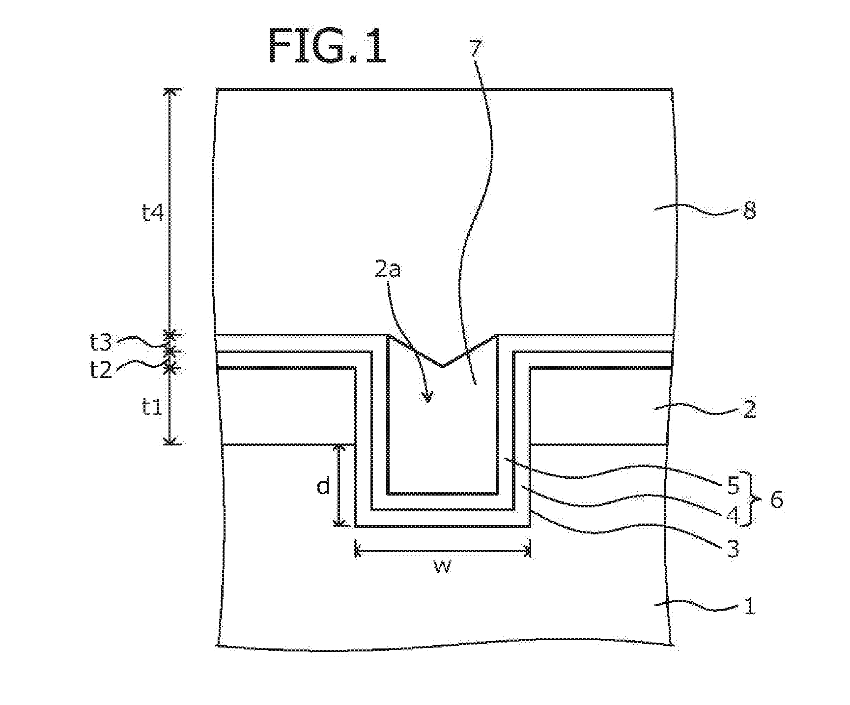
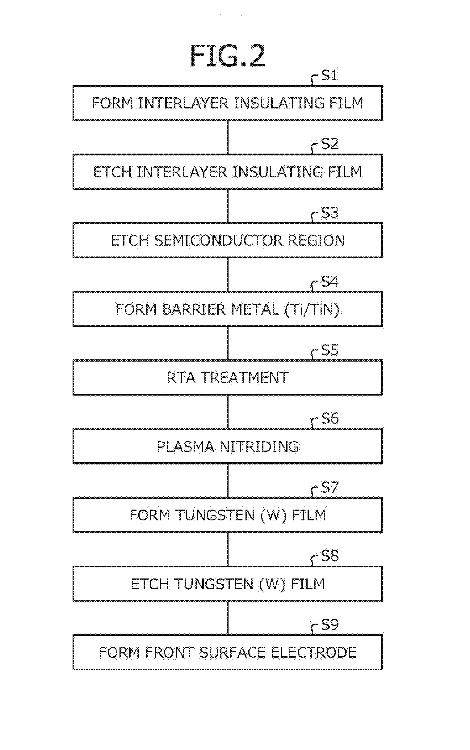
[0032]A case where a contact with a surface electrode that is formed on a substrate surface via an interlayer insulating film is a trench contact will be described as an example of a semiconductor device produced (manufactured) by the method of manufacturing a semiconductor device according to a first embodiment. FIG. 1 is a cross-sectional view of an example of a semiconductor device manufactured by the method of manufacturing a semiconductor device according to the first embodiment. The semiconductor device according to the first embodiment depicted in FIG. 1 includes a trench contact that is a contact with a surface electrode 8 at an inner wall of a trench 3 and formed by embedding, via a barrier metal 6, a plug (extracted portion of electrode) 7 in the trench 3 that is formed in a semiconductor substrate (semiconductor chip) 1. More specifically, for example, on a surface of the semiconductor substrate 1 such as a silicon (Si) substrate, an interlayer insulating film (insulating...
second embodiment
[0044]An example of a semiconductor device produced (manufactured) by the method of manufacturing a semiconductor device according to a second embodiment will be described. FIG. 8 is a cross-sectional view of an example of a semiconductor device manufactured according to the method of manufacturing a semiconductor device according to the second embodiment. A semiconductor device produced by the method of manufacturing a semiconductor device according to the second embodiment differs from a semiconductor device produced by the method of manufacturing a semiconductor device according to the first embodiment in that the trench 3 is not formed in the semiconductor substrate 1. In other words, the surface of the semiconductor substrate 1 is exposed by the contact hole 2a.
[0045]The barrier metal 6 is disposed from the surface of the interlayer insulating film 2 to an inner wall of the contact hole 2a. The barrier metal 6, similar to the first embodiment, is formed by sequentially stackin...
PUM
| Property | Measurement | Unit |
|---|---|---|
| breakdown voltage rating | aaaaa | aaaaa |
| thickness t1 | aaaaa | aaaaa |
| thickness t4 | aaaaa | aaaaa |
Abstract
Description
Claims
Application Information