Ferroelectric random-access memory with pre-patterned oxygen barrier

a random access memory and oxygen barrier technology, applied in the field of semiconductor devices, can solve the problems of reducing the yield of working memories, affecting the performance of working memories, and increasing the cost of fabrication, so as to reduce the cost of fabricating ferroelectric, reduce the cost of ferroelectric, and reduce the defect density

Active Publication Date: 2016-12-01
INFINEON TECH LLC
View PDF2 Cites 16 Cited by
  • Summary
  • Abstract
  • Description
  • Claims
  • Application Information

AI Technical Summary

Benefits of technology

[0008]Non-volatile memory cells including complimentary metal-oxide-semiconductor (CMOS) transistors and embedded ferroelectric capacitors formed according to methods of the present disclosure minimizes changes to the CMOS process flow, reducing cost of fabricating ferroelectric random access memories (F-RAM), lowering defect density and enabling tighter design rules.

Problems solved by technology

Materials and processes typically used to fabricate the CMOS transistors 110, contacts 118 and wiring layer 122 are incompatible with ferroelectric capacitor process flow, and can detrimentally impact their performance.
It will be understood by those skilled in the art that the above described conventional method of fabricating F-RAM undesirably increases an aspect ratio of the ferroelectric capacitors 102, as well as the overall size or height of the F-RAM cell 100, and require several extra mask and processing steps, all of which increase fabrication time, costs, and defect density lowering a yield of working memories.
It has been observed that when a ferroelectric capacitor and / or devices or transistors in the underlying CMOS circuit are exposed to hydrogen introduced, for example, during subsequent processing the properties of the ferroelectric capacitor and / or transistors in the underlying CMOS circuit can be severely degraded.

Method used


Image

  • Ferroelectric random-access memory with pre-patterned oxygen barrier
  • Ferroelectric random-access memory with pre-patterned oxygen barrier
  • Ferroelectric random-access memory with pre-patterned oxygen barrier

Examples


Embodiment Construction

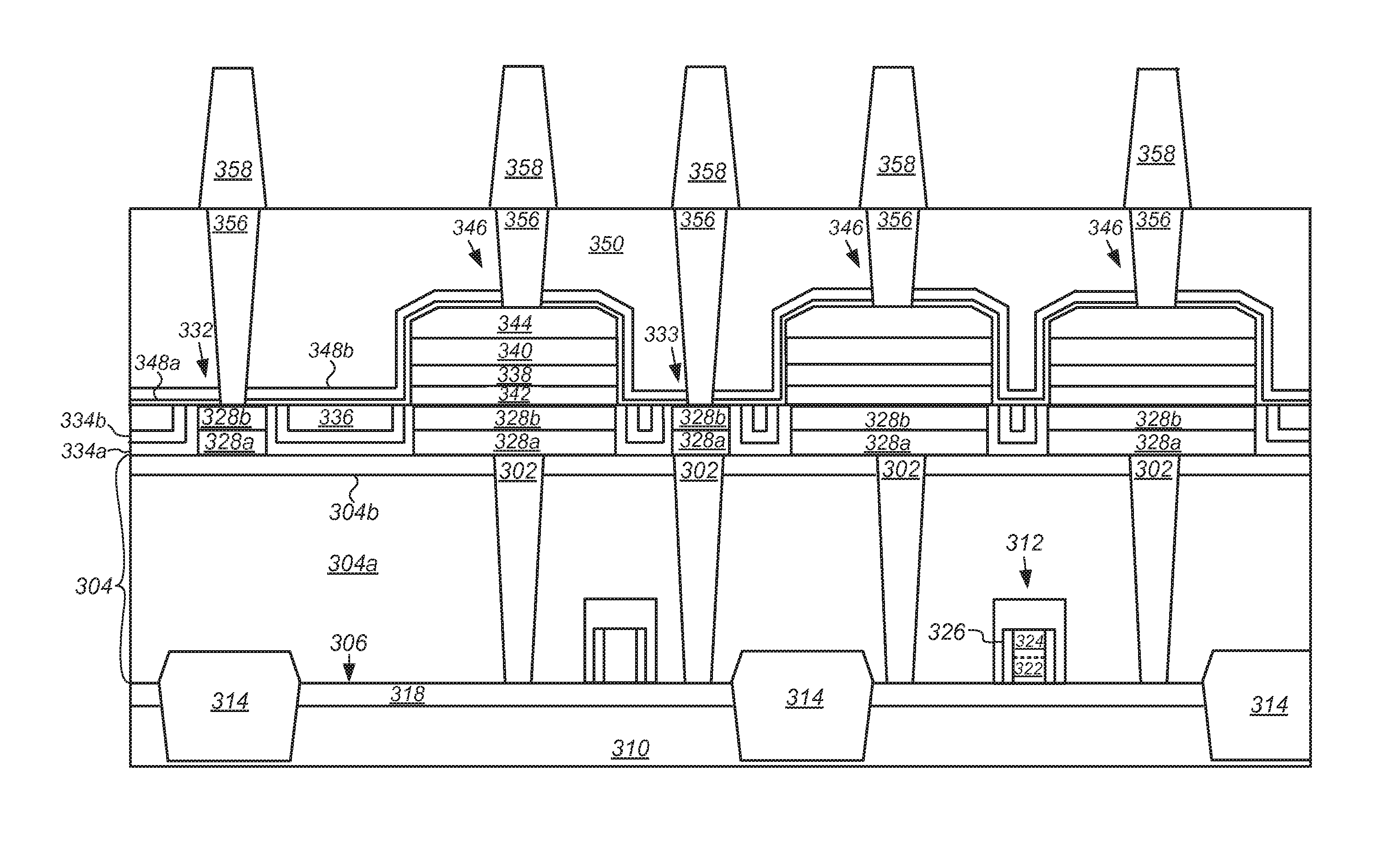
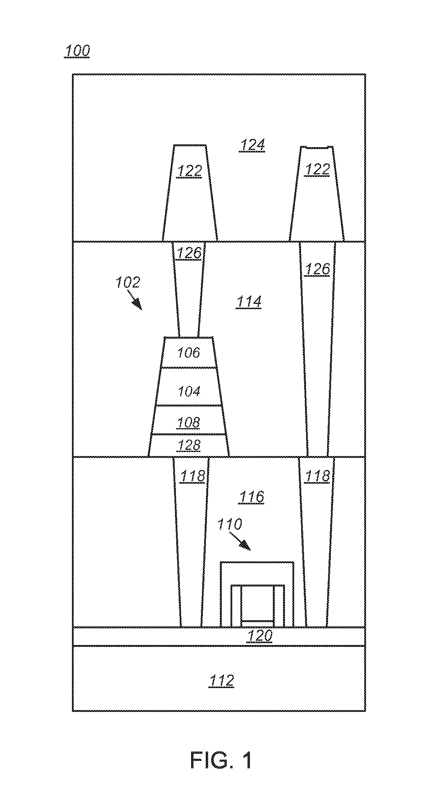
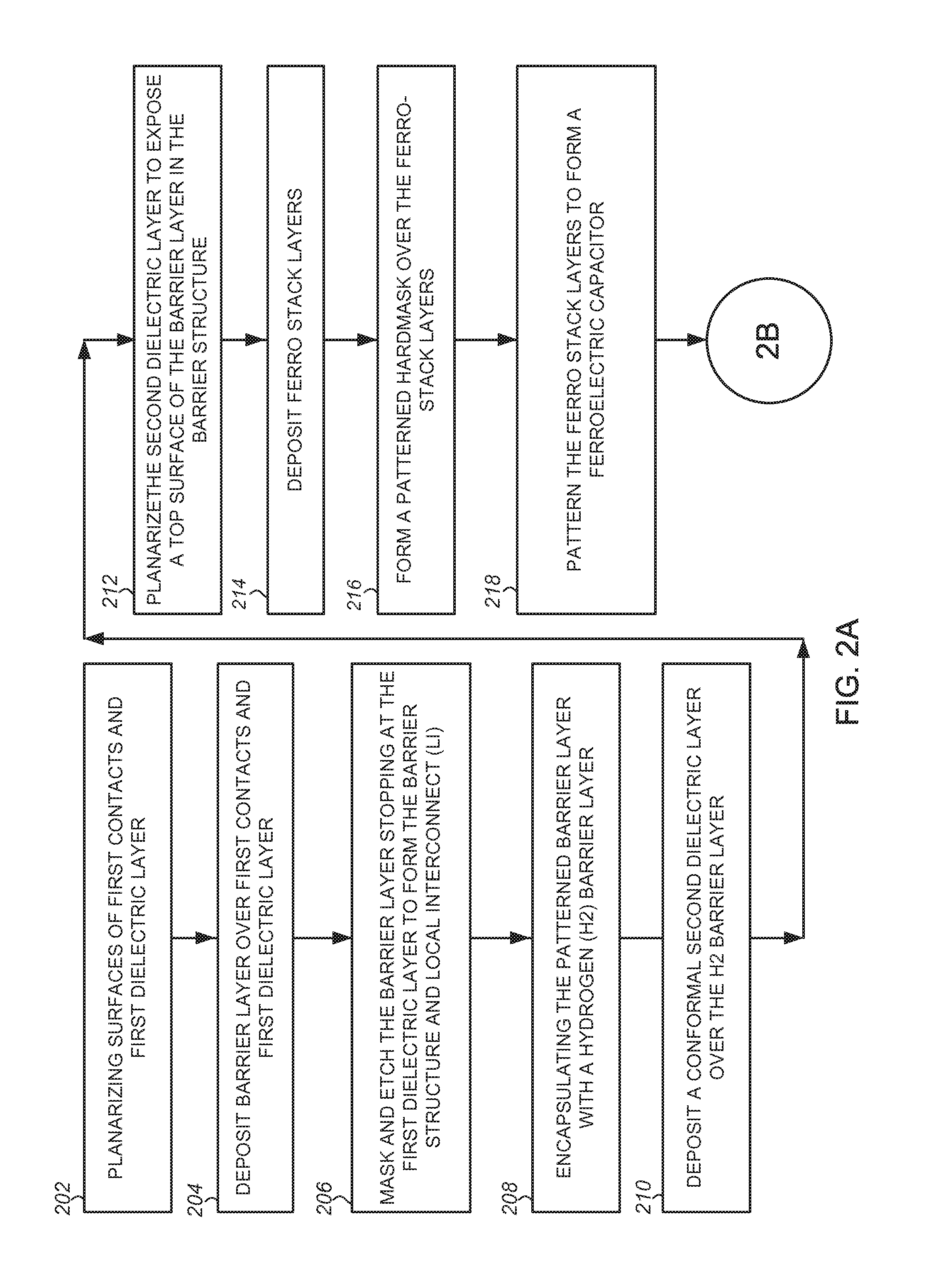
[0020]Embodiments of ferroelectric random access memories (F-RAM) including embedded or integrally formed ferroelectric capacitors and complementary metal-oxide-semiconductor (CMOS) transistors and methods of fabricating the same are described herein with reference to figures. However, particular embodiments may be practiced without one or more of these specific details, or in combination with other known methods, materials, and apparatuses. In the following description, numerous specific details are set forth, such as specific materials, dimensions and processes parameters etc. to provide a thorough understanding of the present invention. In other instances, well-known semiconductor design and fabrication techniques have not been described in particular detail to avoid unnecessarily obscuring the present invention. Reference throughout this specification to “an embodiment” means that a particular feature, structure, material, or characteristic described in connection with the embod...


PUM


Abstract

Structure of F-RAM cells are described. The F-RAM cell include a contact extending through a first dielectric layer on a surface of a substrate. A barrier structure is formed over the contact by depositing and patterning a barrier layer. A second dielectric layer is deposited over the patterned barrier layer and planarized to expose a top surface of the barrier structure. A ferro-stack is deposited and patterned over the barrier structure to form a ferroelectric capacitor. A bottom electrode of the ferroelectric capacitor is electrically coupled to the diffusion region of the MOS transistor through the barrier structure. The barrier layer is conductive so that a bottom electrode of the ferroelectric capacitor is electrically coupled to the contact through the barrier structure. In one embodiment, patterning barrier layer comprises concurrently forming a local interconnect (LI) on a top surface of the first dielectric layer.

Description

CROSS-REFERENCE TO RELATED APPLICATIONS[0001]This application is Continuation application of and claims the benefit of priority to U.S. NonProvisonal patent application Ser. No. 14 / 738,492, filed Jun. 12, 2015, which claims the benefit of priority under 35 U.S.C. 119(e) to U.S. Provisional Patent Application Ser. No. 62 / 169,042, filed Jun. 1, 2015, which are both incorporated by reference herein in each of their entirety.TECHNICAL FIELD[0002]The present disclosure relates generally to semiconductor devices, and more particularly to ferroelectric random access memories (F-RAM) including embedded or integrally formed ferroelectric capacitors and complementary metal-oxide-semiconductor (CMOS) transistors and methods for fabricating the same.BACKGROUND[0003]Ferroelectric random-access memories (F-RAM) typically include a grid or an array of storage elements or cells, each including at least one ferroelectric capacitor and one or more associated transistors to select the cell and control...

Claims


Application Information

Patent Timeline
Patent Type & Authority Applications(United States)
IPC IPC(8): H01L27/115H01L49/02
CPCH01L27/11507H01L28/75H01L28/55H01L28/57H10B53/30H01L28/56
Inventor SUN, SHAN
Owner INFINEON TECH LLC
Why Eureka
Try Eureka