

Reflective mask blank for EUV lithography
a technology of euv and lithography, applied in the field of euv lithography reflection mask blanks, can solve the problems accelerating the miniaturization of semiconductor devices, and the conventional photolithography method is close to its limit, and achieves the effect of deteriorating overlay accuracy
- Summary
- Abstract
- Description
- Claims
- Application Information
AI Technical Summary
Benefits of technology
Problems solved by technology
Method used
Image

Examples
examples
[0112]Now, the present invention will be described in further detail with reference to Examples. However, the present invention is by no means restricted thereto.
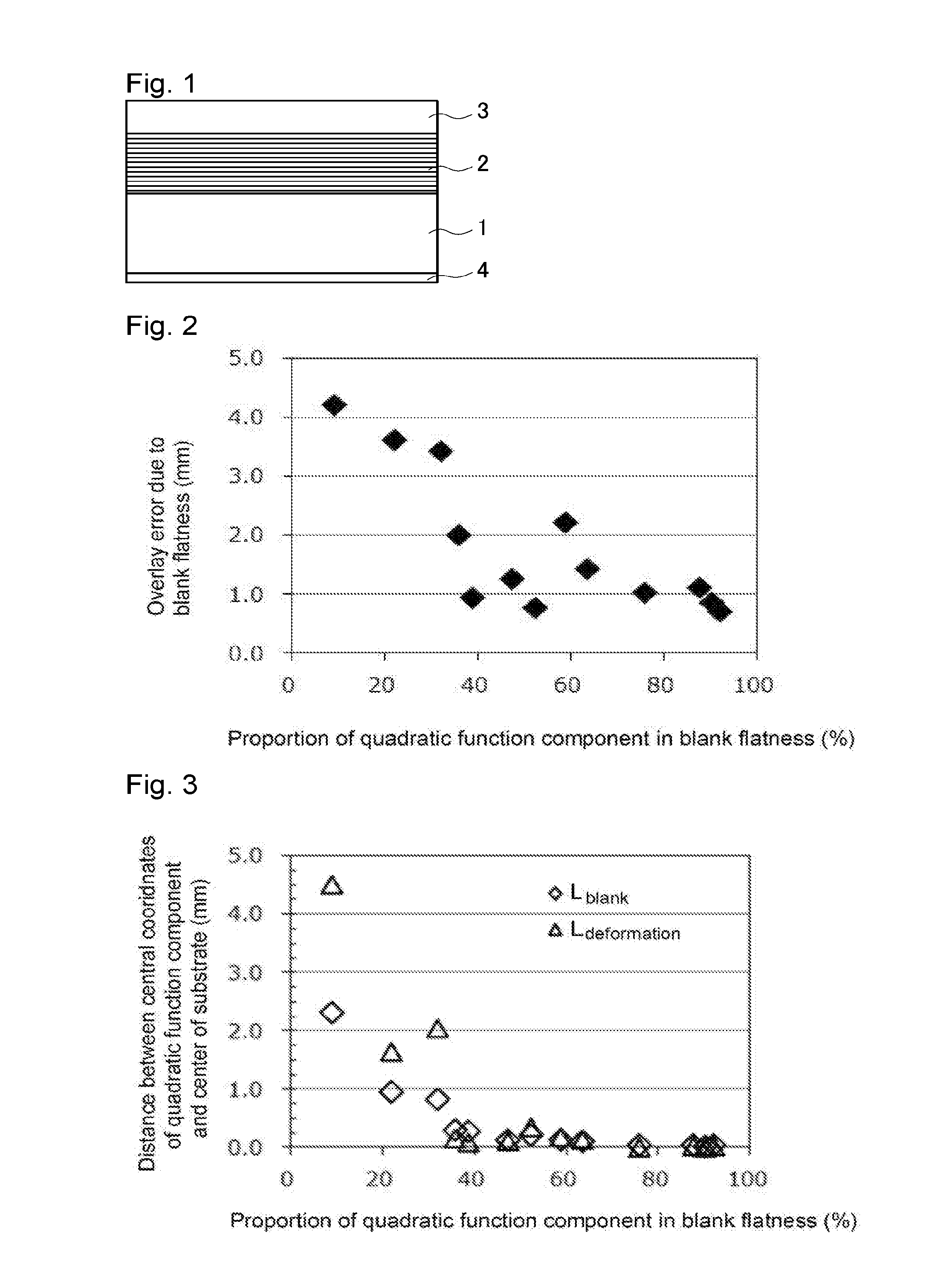
[0113]In this Example, as a substrate 1 for film formation, a SiO2—TiO2 type glass substrate (size: 6 inches (152 mm) square, thickness: 6.35 mm) is used. The quality-guaranteed regions of the main surface and the rear surface of the substrate 1 are measured by a laser interferometer (e.g. “Verifire, Mark IV”, manufactured by Zygo Corporation, “G310S” manufactured by Fujinon Inc. or “FlatMaster” manufactured by Tropel) to obtain the flatness at the quality-guaranteed regions of the main surface and the rear surface. Further, the measured results by the laser interferometer are fitted to quadratic function to obtain the central coordinates F0 and B0 of the quadratic function fitting. The quality-guaranteed region of the main surface of the substrate 1 is a region of 142×142 mm. The quality-guaranteed region of the rear surfa...
PUM
| Property | Measurement | Unit |
|---|---|---|
| flatness | aaaaa | aaaaa |
| flatness | aaaaa | aaaaa |
| wavelength | aaaaa | aaaaa |
Abstract
Description
Claims
Application Information