Check patentability & draft patents in minutes with Patsnap Eureka AI!

Conformal strippable carbon film for line-edge-roughness reduction for advanced patterning

a technology of carbon film and linear edge roughness, applied in the direction of basic electric elements, electrical equipment, semiconductor devices, etc., can solve the problems of reliability loss at the interconnect level in back-end-of-line (beol) applications, leaky transistor failure in front-end-of-line (feol) applications, and the inability of patterning tools designed to create vias or line interconnects 100 nm or more,

Active Publication Date: 2016-12-15
APPLIED MATERIALS INC
View PDF2 Cites 13 Cited by
  • Summary
  • Abstract
  • Description
  • Claims
  • Application Information

AI Technical Summary

Benefits of technology

This patent describes methods and apparatus for decreasing the critical dimensions of a feature formed in a photoresist or hardmask. The methods involve depositing a conformal organic layer directly on the patterned features in the photoresist layer, etching the exposed portion of the hardmask layer to form a recess, and removing the remaining portions of the conformal organic layer and patterned photoresist layer simultaneously using a plasma ashing method. The patent also describes introducing a nitrogen-containing hydrocarbon source and generating a plasma to deposit a conformal organic layer on the patterned features and the exposed portion of the hardmask. Additionally, the patent describes a method of matching the optical properties of the hardmask with the patterned photoresist.

Problems solved by technology

However, due to factors such as optics and light or radiation wavelength, photolithography techniques have a minimum pitch below which a particular photolithographic technique may not reliably form features.
Similarly, patterning tools designed to create vias or line interconnects 100 nm wide or more are not commonly able to create smaller vias.
Therefore, as devices shrink to these small dimensions, current lithography processes are challenged to create patterns with the chosen critical dimensions (CD).
In one example, when considering LER below 14 nm technology node, uncontrolled LER can lead to leaky transistor failure in Front-End-Of-line (FEOL) applications, or reliability loss at the interconnect level in Back-End-Of-Line (BEOL) applications.
However, these approaches decrease throughput and are not cost effective.
Further, the photoresist curing methods recited above do not provide Critical Dimension (CD) shrink.

Method used


Image

  • Conformal strippable carbon film for line-edge-roughness reduction for advanced patterning
  • Conformal strippable carbon film for line-edge-roughness reduction for advanced patterning
  • Conformal strippable carbon film for line-edge-roughness reduction for advanced patterning

Examples


Embodiment Construction

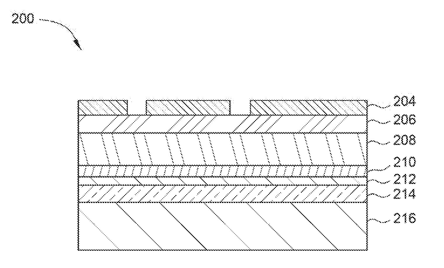
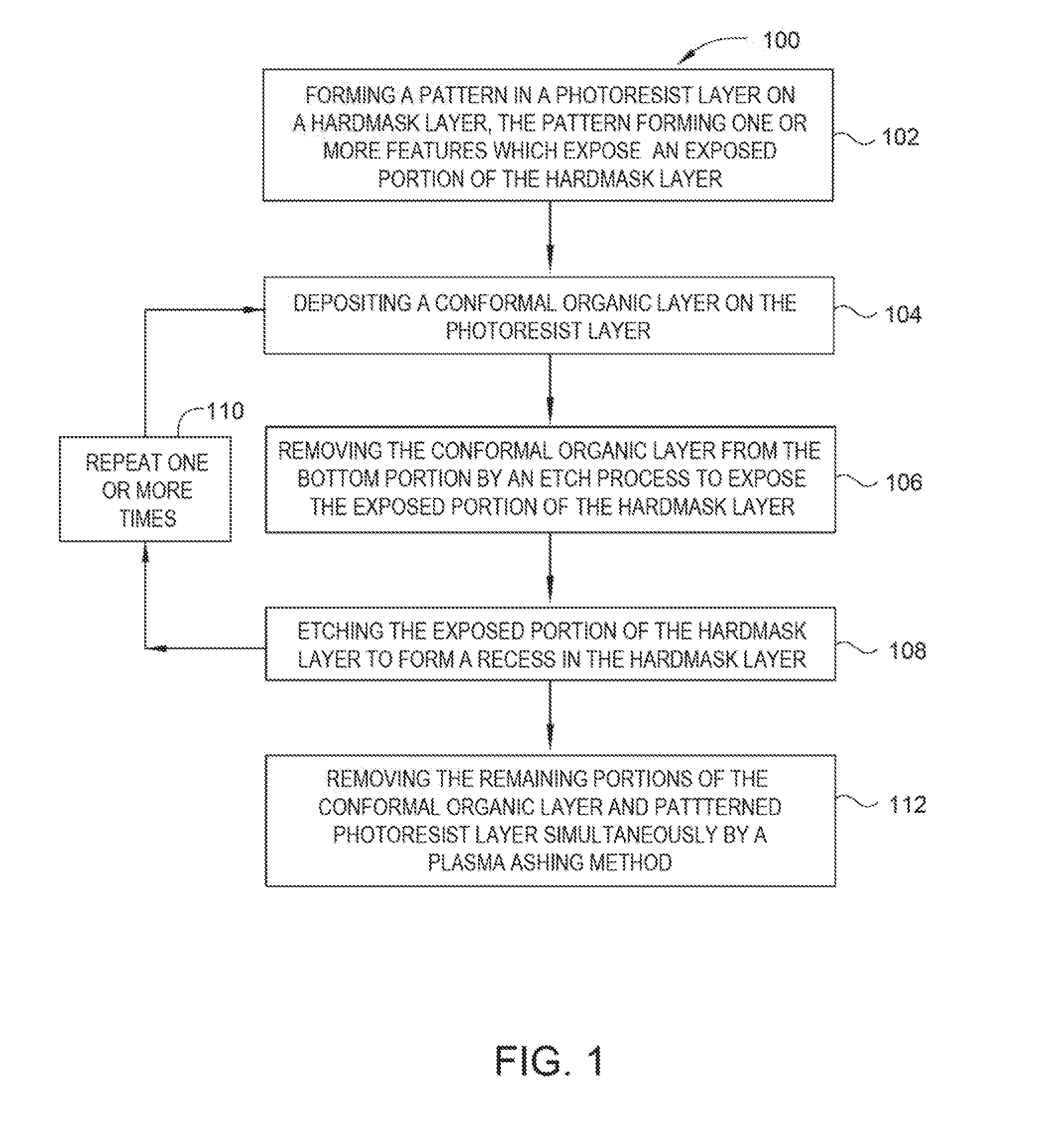
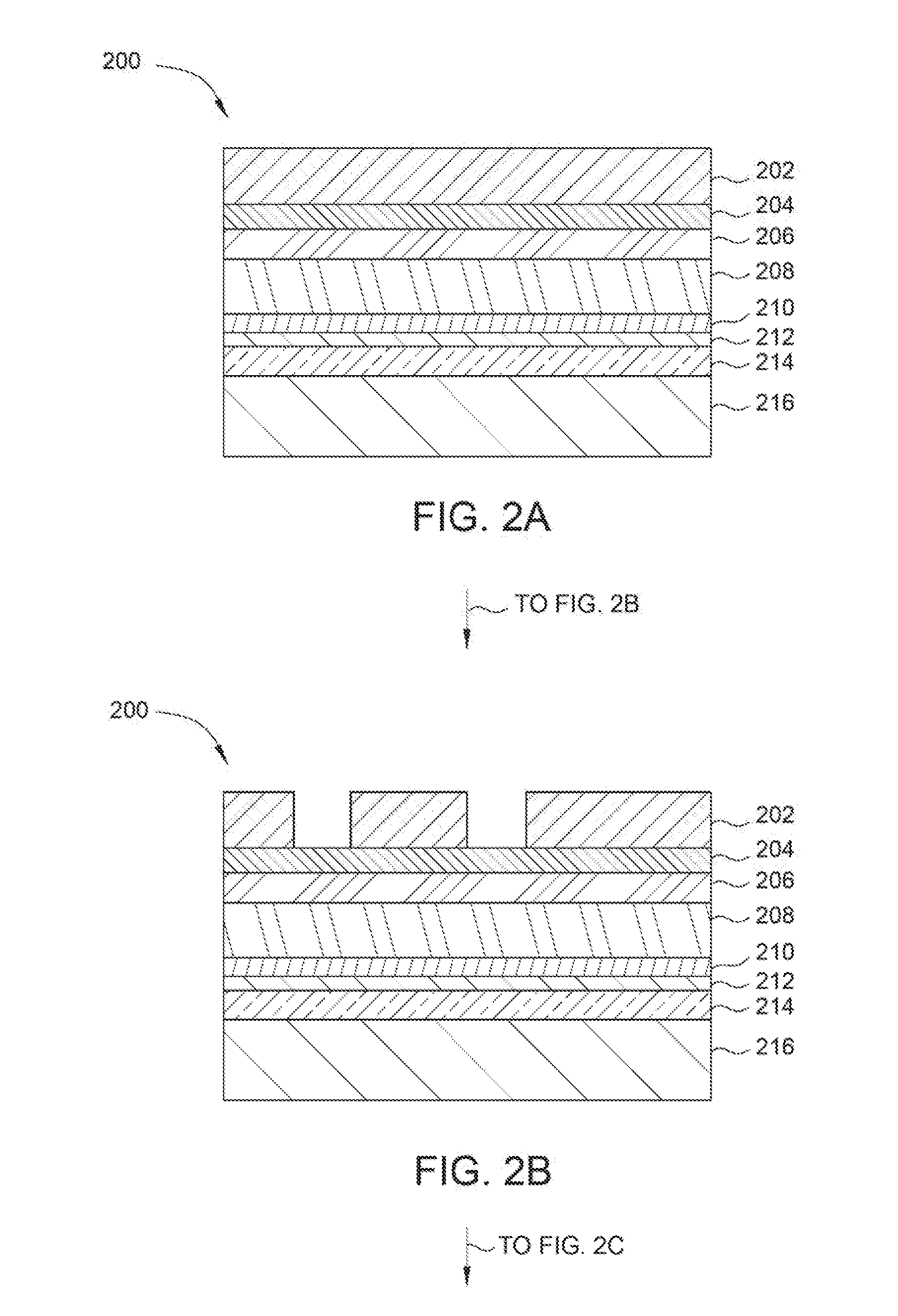
[0016]Embodiments described herein relate to deposition of an ultra-conformal carbon-based material for decreasing the critical dimensions and line edge roughness of a feature formed in a photoresist or a hardmask. In various embodiments, an ultra-conformal carbon-based material is deposited over features formed in a high-resolution photoresist. In one example, a low temperature conformal strippable organic layer (referred to herein as the “conformal organic layer”) may be deposited directly on photoresist. The term “low temperature” described in this disclosure may refer to a temperature range of about 150° C. to about 600° C., for example about 300° C. to about 500° C., such as about 450° C. The photoresist will have features formed therein prior to the deposition. The conformal organic layer formed over the photoresist thus reduces both the CD of the features and the LER of the features, by smoothing edge non-uniformities in the walls of the feature. The conformal organic layer h...


PUM

PropertyMeasurementUnit
temperatureaaaaaaaaaa
refractive indexaaaaaaaaaa

Abstract

Embodiments of the disclosure relate to deposition of a conformal organic material over a feature formed in a photoresist or a hardmask, to decrease the critical dimensions and line edge roughness. In various embodiments, an ultra-conformal carbon-based material is deposited over features formed in a high-resolution photoresist. The conformal organic layer formed over the photoresist thus reduces both the critical dimensions and the line edge roughness of the features.

Description

CROSS-REFERENCE TO RELATED APPLICATIONS[0001]This application claims priority to U.S. provisional patent application Ser. No. 62 / 174,248, filed Jun. 11, 2015, which is herein incorporated by reference.BACKGROUND[0002]Field[0003]The present embodiments generally relate to the fabrication of integrated circuits and particularly to methods for changing critical dimensions of features during an etching process.[0004]Description of the Related Art[0005]Reducing the size of integrated circuits (ICs) results in improved performance, increased capacity and / or reduced cost. Each size reduction requires more sophisticated techniques to form the ICs. Photolithography is commonly used to pattern ICs on a substrate. An exemplary feature of an IC is a line of a material which may be a metal, semiconductor or insulator. Line width is the width of the line and the spacing is the distance between adjacent lines. Pitch is defined as the distance between a same point on two adjacent lines. The pitch i...

Claims


Application Information

Patent Timeline
Patent Type & Authority Applications(United States)
IPC IPC(8): H01L21/033H01L21/3105H01L21/311H01L21/027H01L21/02
CPCH01L21/0337H01L21/0273H01L21/02118H01L21/02266H01L21/31138H01L21/31058H01L21/02274H01L21/02115H01L2221/00
Inventor MEBARKI, BENCHERKIMANNA, PRAMITMIAO, LI YANPADHI, DEENESHKIM, BOK HOENBENCHER, CHRISTOPHER DENNIS
Owner APPLIED MATERIALS INC
Features
  • R&D
  • Intellectual Property
  • Life Sciences
  • Materials
  • Tech Scout
  • Unparalleled Data Quality
  • Higher Quality Content
  • 60% Fewer Hallucinations
Learn More