Microfluidic chip with dielectrophoretic electrodes extending in hydrophilic flow path

a technology of dielectrophoretic electrodes and microfluidic chips, applied in the field of microfluidic chips, can solve the problems of incompatibility with the requirements of microfluidic chip fabrication, manufacturing processes and cost of fabrication, and methods that lack flexibility or operate with limited sample types and flow conditions

Inactive Publication Date: 2016-12-22
IBM CORP
View PDF5 Cites 18 Cited by
  • Summary
  • Abstract
  • Description
  • Claims
  • Application Information

AI Technical Summary

Benefits of technology

[0036]FIG. 6 is a 2D cross-sectional view (partial) of a simplified representation of a microfluidic chip, according to embodiments;
[0037]FIG. 7 is a 2D cross-sectional view (partial) of a simplified representation of a microfluidic chip, comprising a cover sealing microstructures of the chip, according to embodiments;

Problems solved by technology

While several methods and devices for flowing liquids inside microfluidic flow paths have been developed, these methods either lack flexibility or operate with a limited type of samples and flow conditions.
However, contrary to what is done in semiconductor wafer processing, microfluidics generally have deep structures, i.e., around a few micrometer, up to 20 micrometers or even deeper.
In many cases, 5 micrometers is already considered as a small depth in microfluidic applications because such a small depth can generate a large hydraulic resistance on a liquid and can block or become clogged with microbeads and particles, such a small depth can also be incompatible with samples containing cells.
As a result, existing semiconductor wafer processes are challenged by, if not incompatible with the requirements needed for microfluidic chip fabrication both in terms of manufacturing processes and cost of fabrication.

Method used


Image

  • Microfluidic chip with dielectrophoretic electrodes extending in hydrophilic flow path
  • Microfluidic chip with dielectrophoretic electrodes extending in hydrophilic flow path
  • Microfluidic chip with dielectrophoretic electrodes extending in hydrophilic flow path

Examples


embodiments / technical implementation details

3. SPECIFIC EMBODIMENTS / TECHNICAL IMPLEMENTATION DETAILS

3.1 Example of Fabrication Methods

3.1.1 Using Thick Resist / Dry-Film for Microfluidic Structures

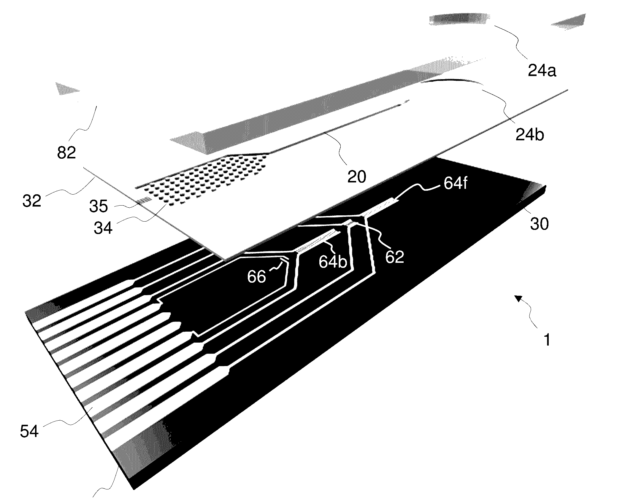
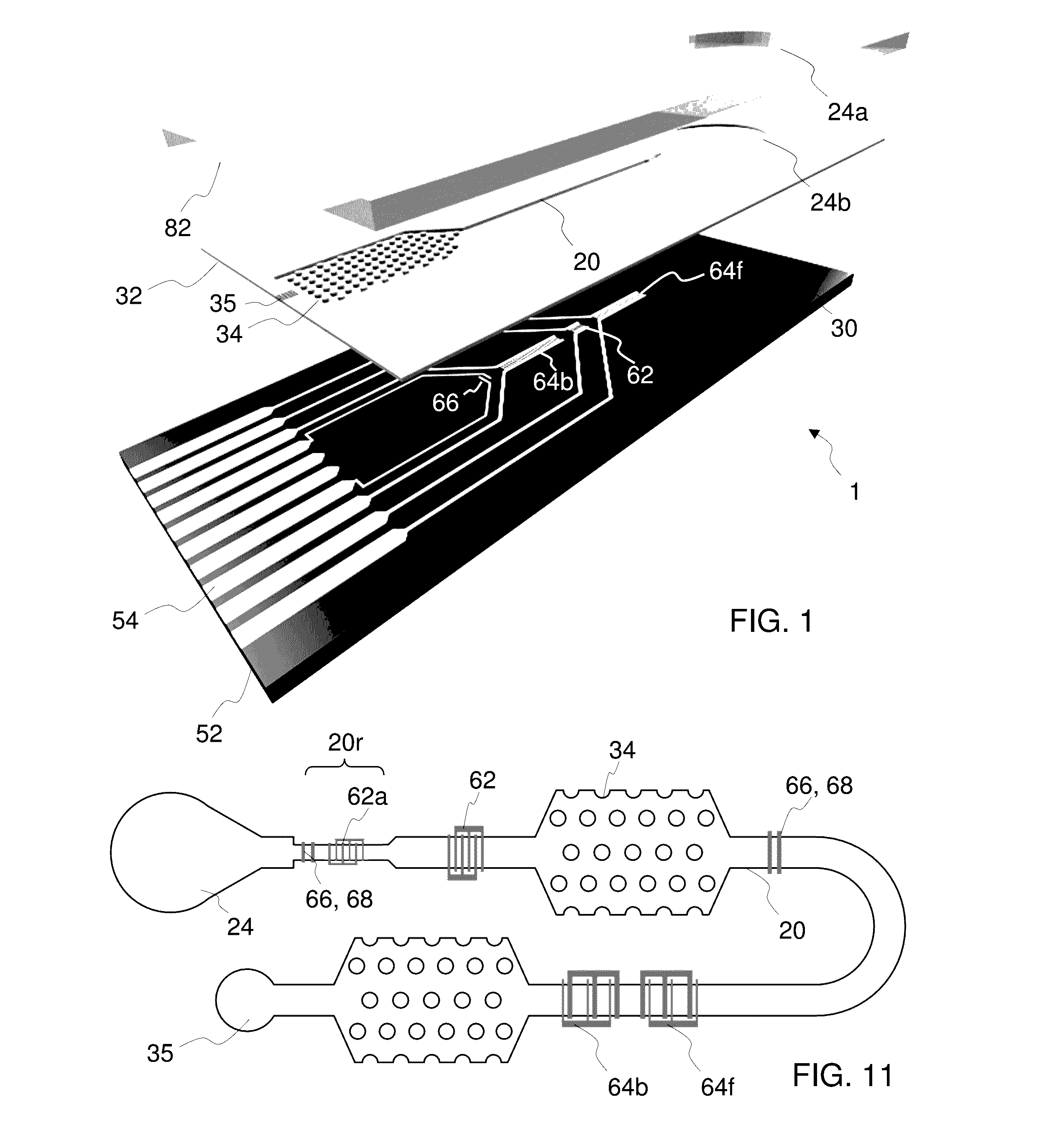
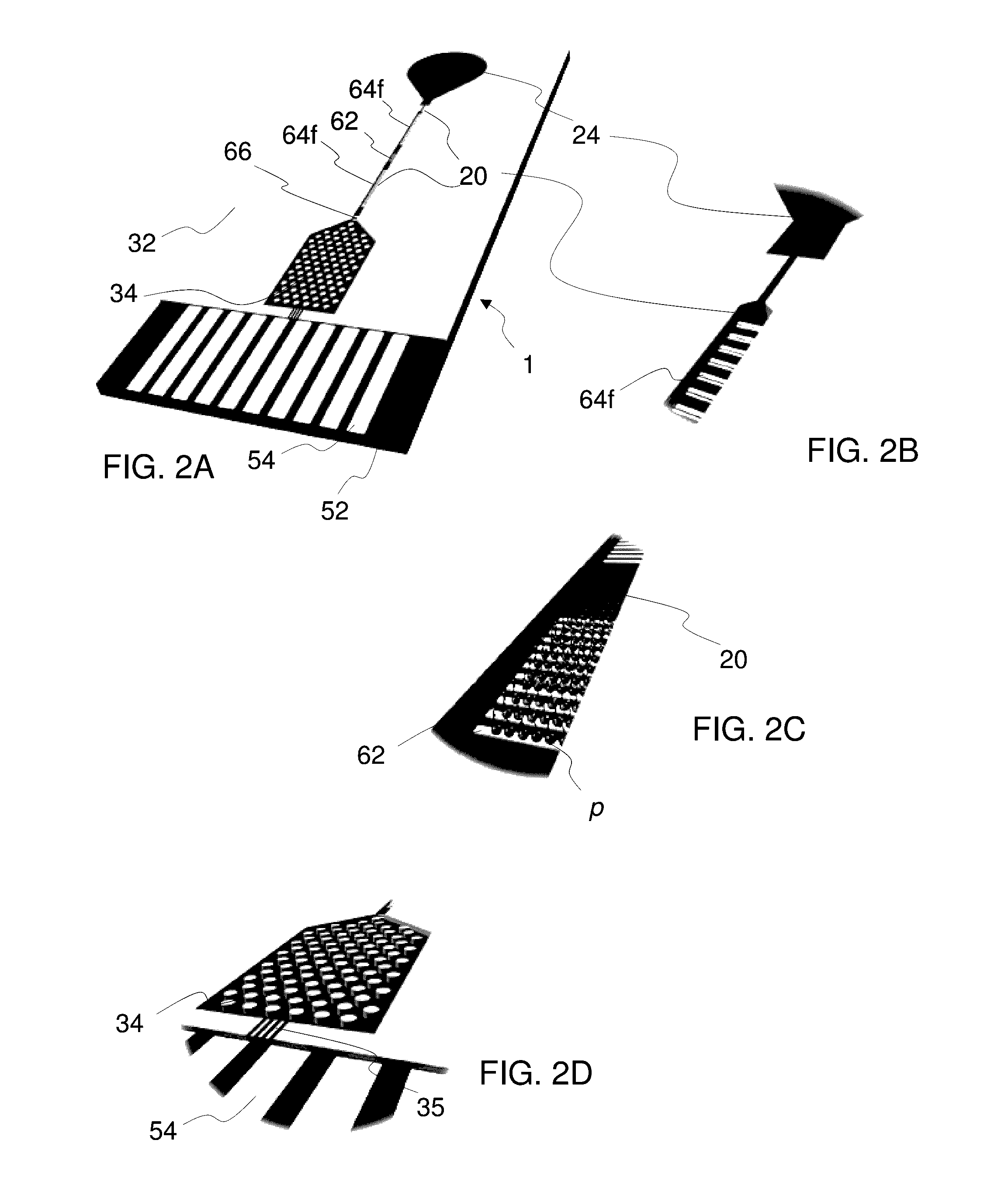
[0134]The substrate can be silicon or glass. Electrodes are patterned on the substrate, e.g., Al (50 nm). Channel patterning is carried out via exposed and developed SU-8 (or dry-film photoresist). The cover can be PDMS, laminate, plastic, etc. The SU-8 is initially hydrophobic, therefore a surface treatment is required, e.g., a 2-3 s cold plasma activation of SU-8 and Si / SiOx chip for achieving hydrophilic surfaces. Such a fabrication provides relatively low resolution and requires quite demanding photolithography steps to eliminate cracks and delamination. A dry-film resist is easier to process and can be initially hydrophilic, i.e. no need for plasma activation. A similar type of dry-film resist can be used to cover the microfluidic structures. Vias (loading pad and air vents) can be on the cover or silicon.

[0135]An example of spec...


PUM

PropertyMeasurementUnit
frequenciesaaaaaaaaaa
frequencyaaaaaaaaaa
particle sizeaaaaaaaaaa

Abstract

The present invention is notably directed to a microfluidic chip (1, 1a) comprising: a flow path (22) defined by a hydrophilic surface; a liquid input (24, 24a, 24b) on one side of the flow path; at least one electrical circuit (62), hereafter DEP circuit, comprising at least one pair of dielectrophoretic electrodes (E21, E22), hereafter DEP electrodes, wherein: each of the DEP electrodes extends transverse to the flow path; and the DEP circuit is configured to generate a dielectrophoretic force, hereafter DEP force, at the level of the DEP electrodes. The chip may further include one or more electroosmotic circuits. The present invention is further directed to methods of operation of such a microfluidic chip.

Description

FIELD OF THE INVENTION[0001]The invention relates in general to the field of microfluidic chips. It is in particular directed to microfluidic chips equipped with dielectrophoretic and electroosmotic circuits, e.g., wafer-based fabricated chips having electrodes extending through microstructures thereof.BACKGROUND OF THE INVENTION[0002]Microfluidics generally refers to microfabricated devices, which are used for pumping, sampling, mixing, analyzing and dosing liquids. Prominent features thereof originate from the peculiar behavior that liquids exhibit at the micrometer length scale. Flow of liquids in microfluidics is typically laminar. Volumes well below one nanoliter can be reached by fabricating structures with lateral dimensions in the micrometer range. Reactions that are limited at large scales (by diffusion of reactants) can be accelerated. Finally, parallel streams of liquids can possibly be accurately and reproducibly controlled, allowing for chemical reactions and gradients ...

Claims


Application Information

Patent Timeline
Patent Type & Authority Applications(United States)
IPC IPC(8): B01L3/00G01N27/447
CPCB01L3/502761B01L3/502707G01N27/44791G01N27/44713G01N27/44743B01L2400/0424B01L2200/0668B01L2300/0877B01L2300/0883B01L2400/0406B01L2400/0418G01N27/44717B03C5/005B03C5/026B03C2201/26
Inventor AZPIROZ, JAIONE TIRAPUDELAMARCHE, EMMANUELGUENZLER, TOBIASKAIGALA, GOVINDTEMIZ, YUKSELTREIBER, TINO
Owner IBM CORP
Why Eureka
Try Eureka