Semiconductor device, manufacturing method thereof, and electronic device

a semiconductor and semiconductor technology, applied in the direction of semiconductor devices, electrical devices, transistors, etc., can solve the problems of significantly affecting transistor characteristics and reliability, increasing becoming more difficult to control the shape of transistors, so as to reduce the parasitic capacitance of transistors, improve the effect of electrical characteristics and high-speed operation

Active Publication Date: 2016-12-22
SEMICON ENERGY LAB CO LTD
View PDF0 Cites 59 Cited by
  • Summary
  • Abstract
  • Description
  • Claims
  • Application Information

AI Technical Summary

Benefits of technology

[0008]Thus, an object of one embodiment of the present invention is to reduce the parasitic capacitance of a transistor. Another object is to provide a semiconductor device capable of high-speed operation. Another object is to provide a semiconductor device with favorable electrical characteristics. Another object is to provide a semiconductor device with high reliability. Another object is to reduce variations in characteristics of a transistor or a semiconductor device that are caused by a manufacturing process. Another object is to provide a semiconductor device ...

Problems solved by technology

However, in miniaturization of transistors, an increase in the parasitic capacitance of transistors is a problem.
Furthermore, it becomes more difficult to control the s...

Method used


Image

  • Semiconductor device, manufacturing method thereof, and electronic device
  • Semiconductor device, manufacturing method thereof, and electronic device
  • Semiconductor device, manufacturing method thereof, and electronic device

Examples


embodiment 1

[0134]In this embodiment, a semiconductor device of one embodiment of the present invention and a manufacturing method of the semiconductor device will be described with reference to drawings.

10>

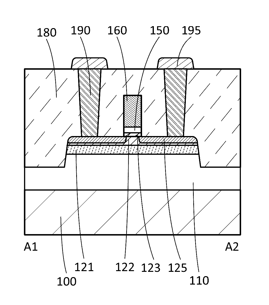
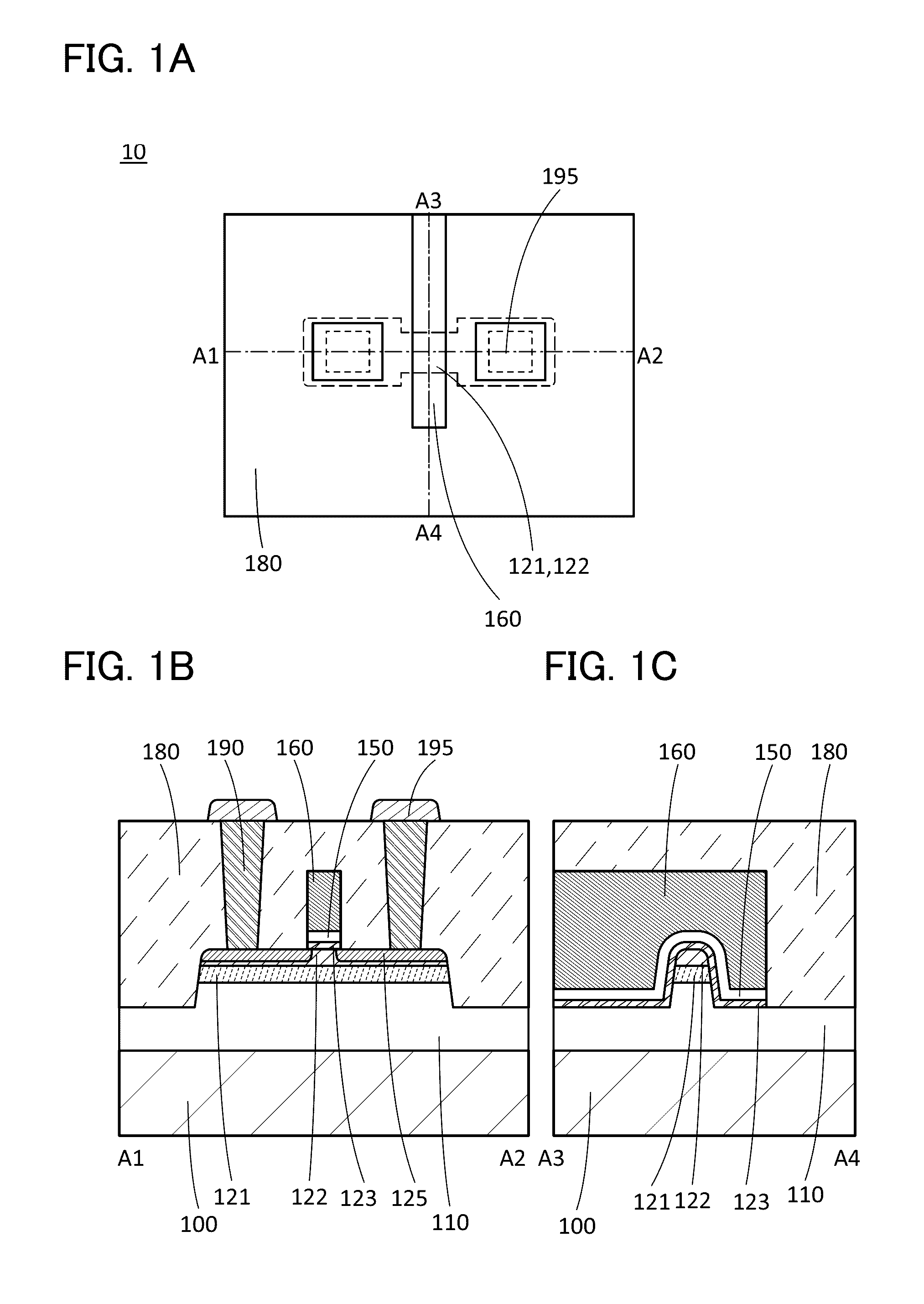
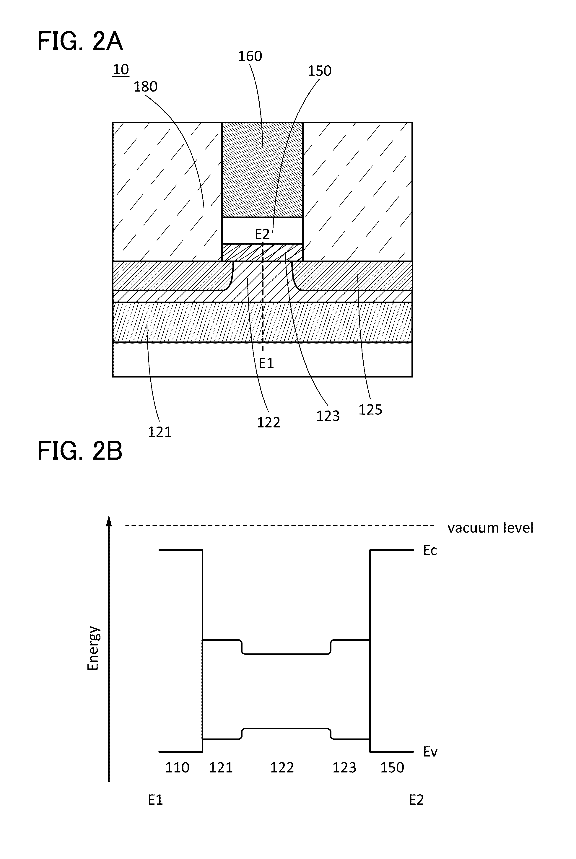
[0135]FIGS. 1A to 1C are a top view and cross-sectional views which illustrate a transistor 10 of one embodiment of the present invention. FIG. 1A is a top view and FIGS. 1B and 1C are cross-sectional views taken along dashed-dotted line A1-A2 and dashed-dotted line A3-A4 in FIG. 1A, respectively. In FIG. 1A, some components are scaled up or down or omitted for simplification of the drawing. In some cases, the direction of dashed-dotted line A1-A2 is referred to as a channel length direction, and the direction of dashed-dotted line A3-A4 is referred to as a channel width direction.

[0136]The transistor 10 includes a substrate 100, an insulating layer 110, a metal oxide layer 121, an oxide semiconductor layer 122, a metal oxide layer 123, a low-resistance region 125, a gate insulating layer 15...

embodiment 2

Structure of Oxide Semiconductor

[0400]The structure of an oxide semiconductor will be described below.

[0401]An oxide semiconductor is classified into a single crystal oxide semiconductor and a non-single-crystal oxide semiconductor. Examples of a non-single-crystal oxide semiconductor include a c-axis aligned crystalline oxide semiconductor (CAAC-OS), a polycrystalline oxide semiconductor, a nanocrystalline oxide semiconductor (nc-OS), an amorphous-like oxide semiconductor (a-like OS), and an amorphous oxide semiconductor.

[0402]From another perspective, an oxide semiconductor is classified into an amorphous oxide semiconductor and a crystalline oxide semiconductor. Examples of a crystalline oxide semiconductor include a single crystal oxide semiconductor, a CAAC-OS, a polycrystalline oxide semiconductor, and an nc-OS.

[0403]An amorphous structure is generally thought to be isotropic and have no non-uniform structure, to be metastable and have no fixed positions of atoms, to have a fl...

embodiment 3

[0485]In this embodiment, an example of a circuit including the transistor of one embodiment of the present invention will be described with reference to drawings.

[0486]FIG. 42A is a cross-sectional view of a semiconductor device of one embodiment of the present invention. In FIG. 42A, the X1-X2 direction and the Y1-Y2 direction represent a channel length direction and a channel width direction, respectively. The semiconductor device illustrated in FIG. 42A includes a transistor 2200 using a first semiconductor material in a lower portion and a transistor 2100 using a second semiconductor material in an upper portion. In FIG. 42A, an example is described in which the transistor described in the above embodiment as an example is used as the transistor 2100 using the second semiconductor material. A cross-sectional view of the transistors in a channel length direction is on the left side of a dashed-dotted line, and a cross-sectional view of the transistors in a channel width directio...


PUM


Abstract

A semiconductor device includes a first insulating layer over a substrate, a first metal oxide layer over the first insulating layer, an oxide semiconductor layer over the first metal oxide layer, a second metal oxide layer over the oxide semiconductor layer, a gate insulating layer over the second metal oxide layer, a second insulating layer over the second metal oxide layer, and a gate electrode layer over the gate insulating layer. The gate insulating layer includes a region in contact with a side surface of the gate electrode layer. The second insulating layer includes a region in contact with the gate insulating layer. The oxide semiconductor layer includes first to third regions. The first region includes a region overlapping with the gate electrode layer. The second region, which is between the first and third regions, includes a region overlapping with the gate insulating layer or the second insulating layer. The second and third regions each include a region containing an element N (N is phosphorus, argon, or xenon).

Description

TECHNICAL FIELD[0001]The present invention relates to an object, a method, or a manufacturing method. In addition, the present invention relates to a process, a machine, manufacture, or a composition of matter. In particular, the present invention relates to, for example, a semiconductor device, a display device, a light-emitting device, a power storage device, an imaging device, a driving method thereof, or a manufacturing method thereof. In particular, one embodiment of the present invention relates to a semiconductor device or a method for manufacturing the semiconductor device.[0002]In this specification and the like, a semiconductor device generally means a device that can function by utilizing semiconductor characteristics. A transistor and a semiconductor circuit are embodiments of semiconductor devices. In some cases, a memory device, a display device, or an electronic device includes a semiconductor device.BACKGROUND ART[0003]A technique by which a transistor is formed usin...

Claims


Application Information

Patent Timeline
IPC IPC(8): H01L29/786H01L27/12H01L21/425H01L21/46H01L29/04H01L29/66
CPCH01L29/78693H01L29/045H01L29/7869H01L27/1262H01L21/425H01L21/46H01L29/66969H01L29/24H01L29/42384H01L29/4908H01L29/7782H01L29/7854H01L29/7855H01L29/78618H01L29/78648H01L29/78696H01L27/1207H01L27/1225
Inventor ITO, DAIGOMATSUBAYASHI, DAISUKENAGAI, MASAHARUYAMAMOTO, YOSHIAKIHAMADA, TAKASHIOKAZAKI, YUTAKASASAGAWA, SHINYAKURATA, MOTOMUYAMADE, NAOTO
Owner SEMICON ENERGY LAB CO LTD
Why Eureka
Try Eureka