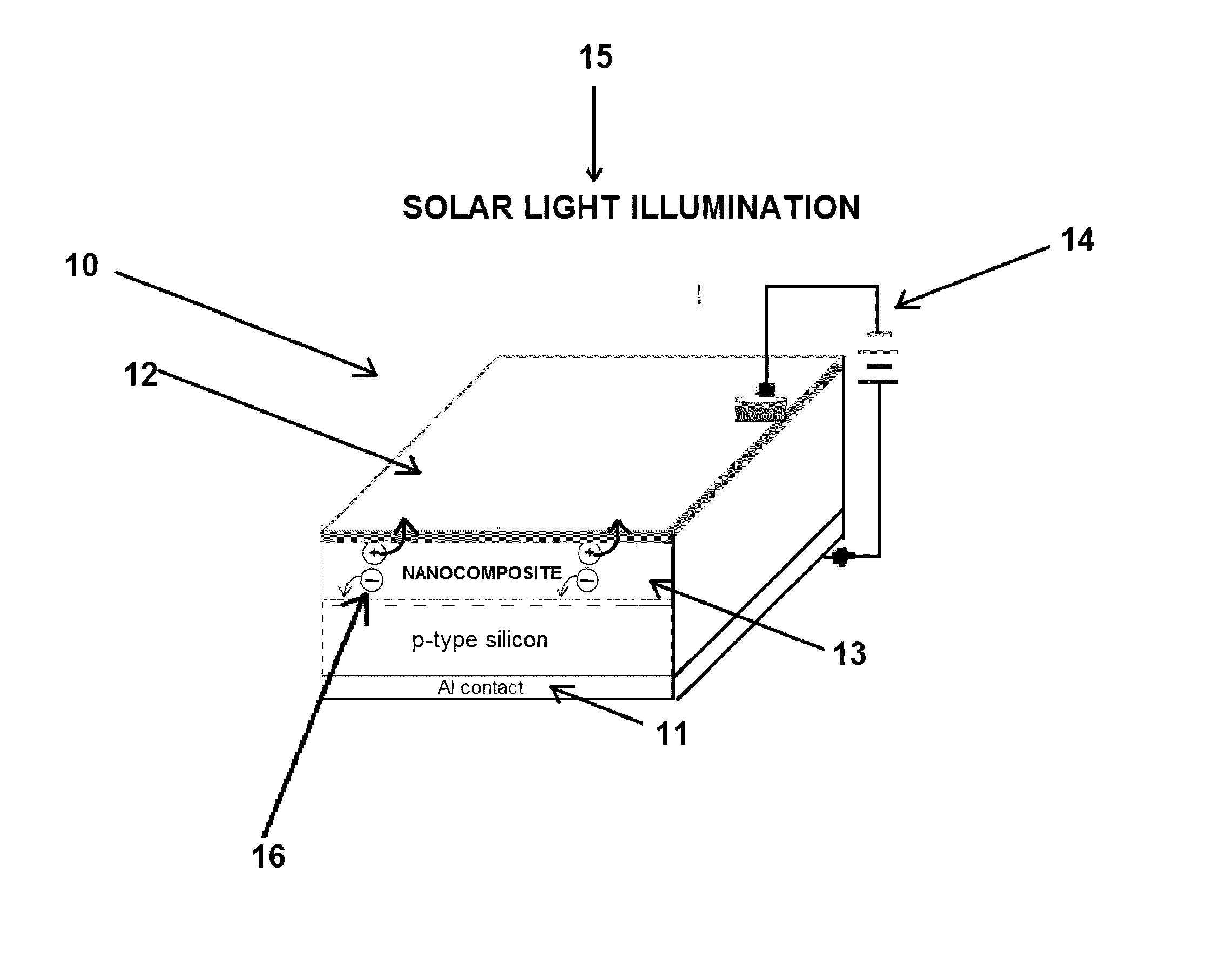
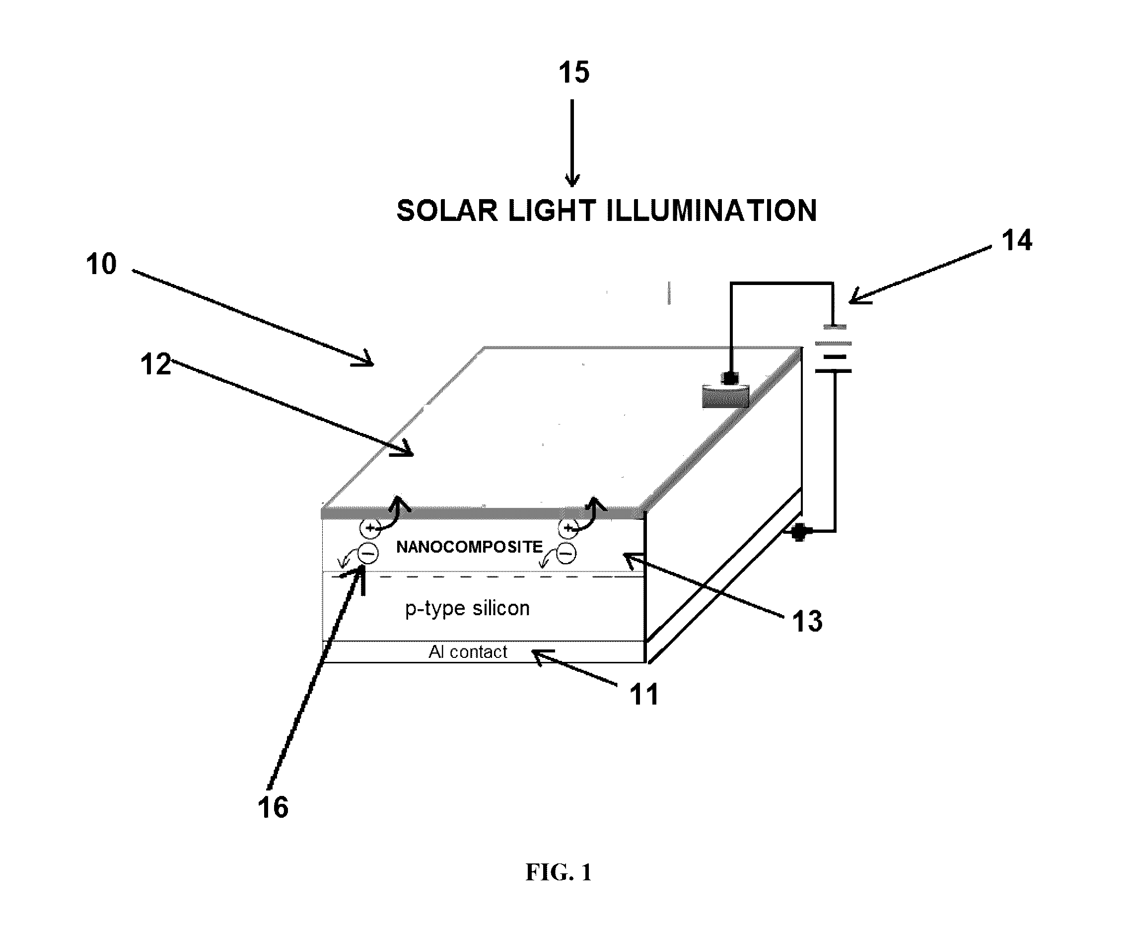
Single layer nanocomposite photoresponse device
- Summary
- Abstract
- Description
- Claims
- Application Information
AI Technical Summary
Benefits of technology
Problems solved by technology
Method used
Image

Examples
example 1
Preparation of ZnO Nanoparticles and the Photoactive Nanocomposite Layer
[0137]The chemicals used in various embodiments of the present invention were supplied by Aldrich company as analytical grade reagents. The raw materials were used as purchased without further purification. Millipore MilliQ purified deionized water was used in all operations.
[0138]An aqueous solution of 50 mL total volume containing 0.25 mol of zinc nitrate hexahydrate, Zn(NO3)2.6H2O, and 0.4 mol urea was prepared at room temperature. The mixture was vigorously magnetically stirred for 10 min and then transferred to a Teflon-lined steel autoclave of 50 mL capacity. The steel autoclave was sealed and the hydrothermal cell kept at 220° C. for 3 h. After the cooling of the autoclave to room temperature solid product of naturally white precipitates were filtered and rinsed with water up to pH=7. The obtained powders were dried in an oven at 80° C. overnight.
[0139]Subsequently, the synthesized ZnO nanorods were dispe...
example 2
Characterizations of the Prepared ZnO Nanoparticles and the Photoactive Nanocomposite Layer
[0140]The results obtained from a variety of relevant instrumental studies of the as synthesized pure ZnO nanoparticles and photoactive nanocomposite layer, to offer insights into the morphology and electrical properties, are laid out in the following examples.
example 3
X-Ray Diffraction (XRD) Analysis of the Prepared ZnO Nanoparticles
[0141]The crystal structure of ZnO nanoparticles was characterized by X-Ray diffraction (XRD) with Cu Kα radiation (λ=0.15418 nm). FIG. 3 shows XRD patterns of ZnO nanoparticles. The peaks at 2θ=31.67°, 34.31°, 36.14°, 47.40°, 56.52°, 62.73°, 66.28°, 67.91°, 69.03°, and 72.48° were assigned to (100), (002), (101), (102), (110), (103), (200), (112), (201), and (004) of ZnO nanoparticles, indicating that the samples were polycrystalline wurtzite structure (Zincite, JCPDS 5-0664). No characteristic peaks of any impurities were detected, suggesting that high-quality ZnO nanoparticles were synthesized.
PUM
 Abstract
Description
Claims
Application Information
 - R&D
- Intellectual Property
- Life Sciences
- Materials
- Tech Scout
- Unparalleled Data Quality
- Higher Quality Content
- 60% Fewer Hallucinations
Browse by: Latest US Patents, China's latest patents, Technical Efficacy Thesaurus, Application Domain, Technology Topic, Popular Technical Reports.
© 2025 PatSnap. All rights reserved.Legal|Privacy policy|Modern Slavery Act Transparency Statement|Sitemap|About US| Contact US: help@patsnap.com