
Thin Film Transistor Array Substrate and Manufacturing Method Thereof

Active Publication Date: 2017-01-19
TCL CHINA STAR OPTOELECTRONICS TECH CO LTD
View PDF0 Cites 1 Cited by
  • Summary
  • Abstract
  • Description
  • Claims
  • Application Information

AI Technical Summary

Benefits of technology

This patent is about a way to make sure that thin film transistors (the important components in LCD display panels) don't change their voltage threshold when they are exposed to negative bias illumination stress. This improves the reliability of the thin film transistors and results in better quality LCD display panels.

Problems solved by technology

However, under the situation of negative bias illumination stress (NBIS), the threshold voltage of the a-IGZO TFT is easily to drift.
Therefore it is difficult for the a-IGZO TFT to achieve large-scale production.

Method used


Image

  • Thin Film Transistor Array Substrate and Manufacturing Method Thereof
  • Thin Film Transistor Array Substrate and Manufacturing Method Thereof
  • Thin Film Transistor Array Substrate and Manufacturing Method Thereof

Examples


Embodiment Construction

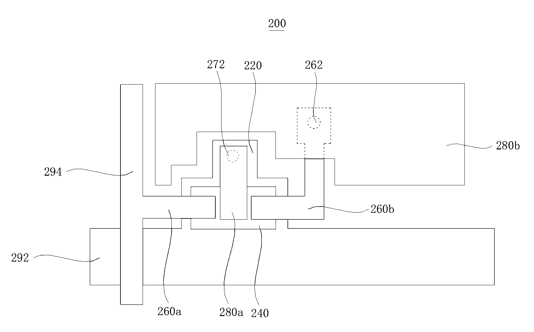
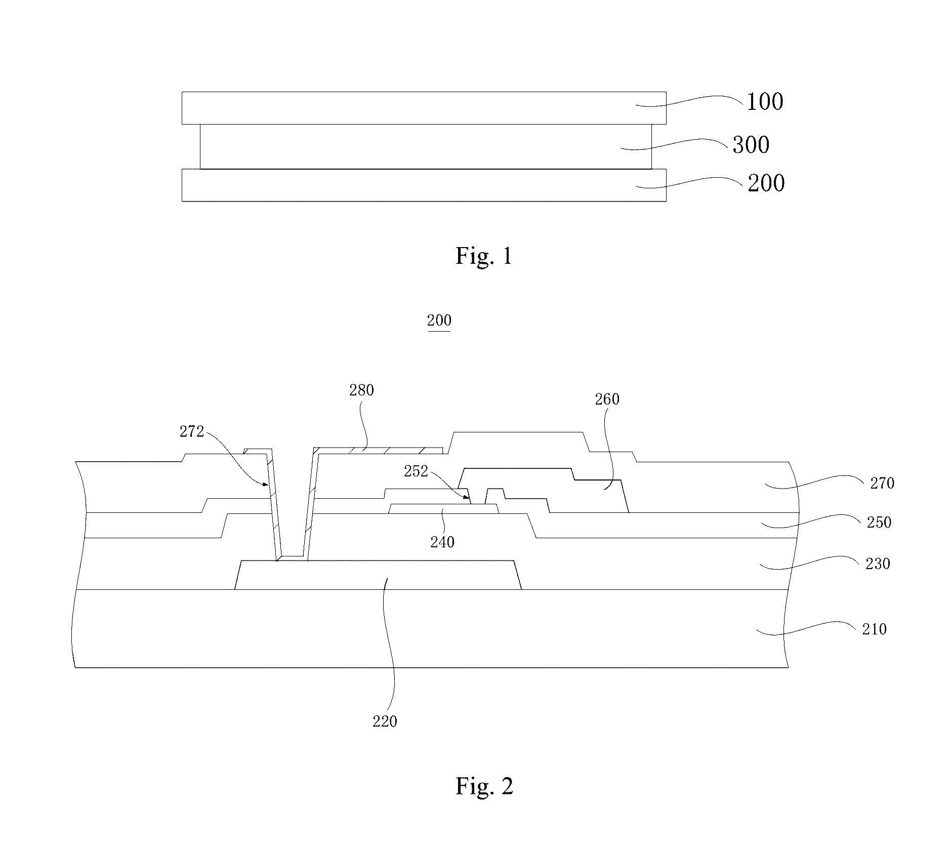
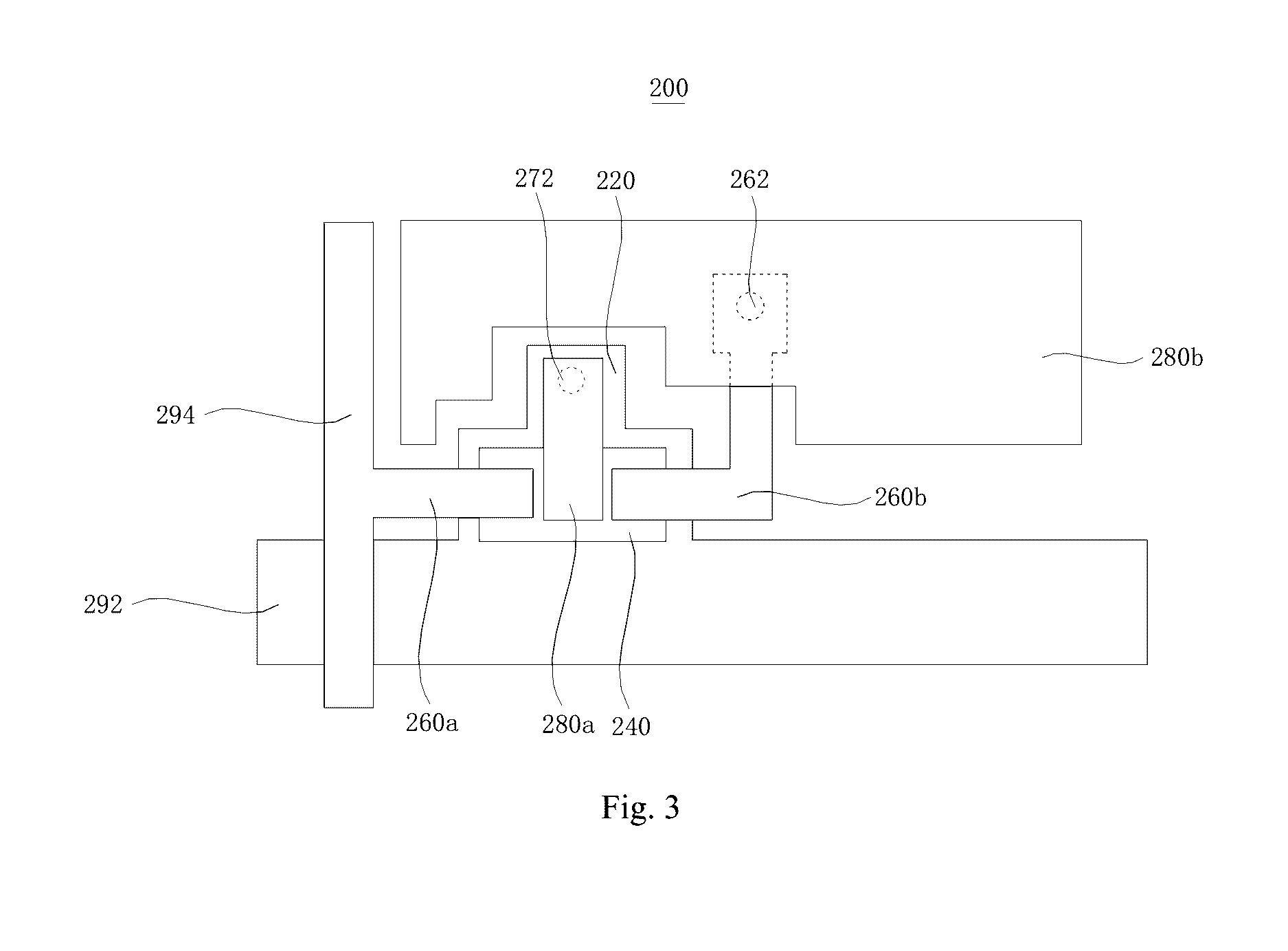
[0027]Hereinafter, embodiments of the disclosure will be described in detail with the accompanying drawings. However, the disclosure may be achieved in many different forms, and the disclosure should not be construed as limited to the specific embodiments set forth herein. Rather, these embodiments are provided to explain the principles of the invention and its practical application, so that others skilled in the art may understand the invention for various embodiments and various modifications suited to the particular intended application. In the drawings, in order to clearly illustrate the component, the thickness of layers and regions are exaggerated. The same reference numerals throughout the specification and drawings can be used to denote the same elements. It also should be understood that when a layer or element is referred to as being formed “on” another layer or substrate, it can be formed directly on the other layer or substrate, or intermediate layers may also be present...


PUM


Abstract

A thin film transistor array substrate comprises a bottom gate disposed on a substrate and a bottom gate insulating layer covering the bottom gate, a semiconductor oxide layer disposed on the bottom gate insulating layer and an etch blocking layer covering the semiconductor oxide layer and including a first via, a drain disposed on the etch blocking layer contacting with the semiconductor oxide layer through the first via and an insulating protection layer covering the drain, a second via arranged in the insulating protection layer, the etch blocking layer and the bottom gate insulating layer, a top gate disposed on insulating protection layer contacting with the bottom gate through the second via. The disclosure further discloses a method for manufacturing a thin film transistor array substrate. The thin film transistor of the disclosure prevents the threshold voltage thereof from being drifted in a case of negative bias illumination stress (NBIS).

Description

BACKGROUND[0001]Technical Field[0002]The disclosure is related to display technology field, and more particular to a thin film transistor array substrate and a manufacturing method thereof being able to prevent the threshold voltage (Vth) from drifting in a case of the negative bias illumination stress (NBIS).[0003]Related Art[0004]With the evolution of optical and semiconductor technology, the flat panel display has been flourishing. Among the various flat panel displays, the liquid crystal display (abbreviated LCD) has become the mainstream on the market due to due to the various superior characteristics such as the high space utilization efficiency, low power consumption, no radiation and low electromagnetic interference.[0005]The liquid crystal display device usually comprises a liquid crystal display panel and a backlight module arranged opposite to each other. The backlight module provides display light to the liquid crystal display panel. The liquid crystal display panel usua...

Claims


Application Information

Patent Timeline
IPC IPC(8): G02F1/1368H01L29/786G02F1/1362H01L29/66G02F1/1343H01L27/12H01L29/49
CPCG02F1/1368H01L27/1248H01L29/78648H01L29/78633H01L29/4908H01L29/78693G02F2202/10G02F1/13439G02F1/136227G02F1/136209G02F2001/13685G02F2201/123H01L29/66969H01L27/124H01L27/1225G02F1/13685G02F1/133345
Inventor XU, XIANGYANG
Owner TCL CHINA STAR OPTOELECTRONICS TECH CO LTD
Learn More