Wafer thinning method

a thinning method and a technology of abrasive members, applied in the field of thinning methods, can solve the problems of poor economy, abrasive members may wear in an amount of approximately 4 times, etc., and achieve the effects of suppressing the wear amount of abrasive members, reducing the thickness of wafers, and suppressing damage to the first wafers

Active Publication Date: 2017-01-26
DISCO CORP
View PDF8 Cites 24 Cited by
  • Summary
  • Abstract
  • Description
  • Claims
  • Application Information

AI Technical Summary

Benefits of technology

[0011]According to the wafer thinning method of the present invention, the modified layers and the cracks are formed inside the wafer in the central area surrounded by the annular groove. Thereafter, an external force is applied to the wafer to thereby separate the wafer into two wafers, that is, the first wafer and the second wafer at the separation start point (along a separation plane) composed of the modified layers and the cracks. Accordingly, the thickness of the wafer can be easily reduced to the finished thickness of the wafer after thinning as the thickness of the first wafer having the first surface on which the plural devices are formed. Accordingly, the wafer formed from the SiC substrate can be thinned without grinding the back side of the wafer by using abrasive members, so t

Problems solved by technology

Accordingly, in grinding the back side of a wafer formed from an SiC substrate by using a grinding wheel having abrasive members, there is a problem

Method used


Image

  • Wafer thinning method
  • Wafer thinning method
  • Wafer thinning method

Examples


Embodiment Construction

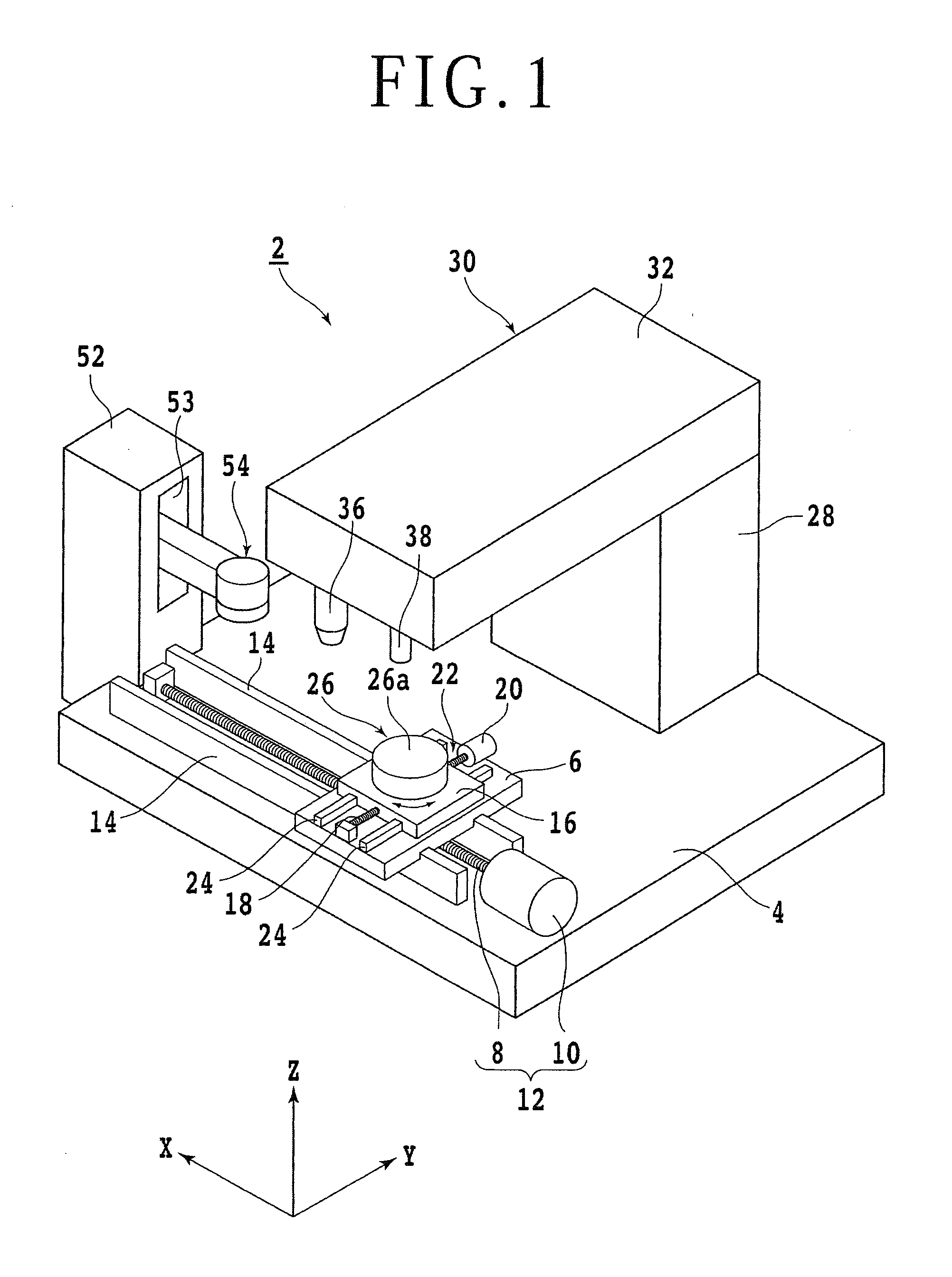
[0032]A preferred embodiment of the present invention will now be described in detail with reference to the drawings. Referring to FIG. 1, there is shown a perspective view of a laser processing apparatus 2 suitable for use in performing a wafer thinning method of the present invention. The laser processing apparatus 2 includes a stationary base 4 and a first slide block 6 mounted on the stationary base 4 so as to be movable in the X direction. The first slide block 6 is moved in a feeding direction, or in the X direction along a pair of guide rails 14 by a feeding mechanism 12 composed of a ball screw 8 and a pulse motor 10.

[0033]A second slide block 16 is mounted on the first slide block 6 so as to be movable in the Y direction. The second slide block 16 is moved in an indexing direction, or in the Y direction along a pair of guide rails 24 by an indexing mechanism 22 composed of a ball screw 18 and a pulse motor 20. A chuck table 26 having a suction holding portion 26a is mounted...


PUM


Abstract

Disclosed herein is a wafer thinning method for thinning a wafer formed from an SiC substrate having a first surface and a second surface opposite to the first surface. The wafer thinning method includes an annular groove forming step of forming an annular groove on the second surface of the SiC substrate in an annular area corresponding to the boundary between a device area and a peripheral marginal area in the condition where a thickness corresponding to the finished thickness of the wafer after thinning is left, and a separation start point forming step of applying the laser beam to the second surface as relatively moving a focal point and the SiC substrate to thereby form a modified layer and cracks inside the SiC substrate at the predetermined depth.

Description

BACKGROUND OF THE INVENTION[0001]1. Field of the Invention[0002]The present invention relates to a wafer thinning method for thinning a wafer composed of an SiC substrate and a plurality of devices formed on the front side of the SiC substrate.[0003]2. Description of the Related Art[0004]Various devices such as integrated circuits (ICs) and large-scale integrations (LSIs) are formed by forming a functional layer on the front side of a wafer formed from a silicon substrate and partitioning this functional layer into a plurality of regions along a plurality of crossing division lines. The back side of the wafer is ground by a grinding apparatus to thereby reduce the thickness of the wafer to a predetermined thickness. Thereafter, the division lines of the wafer are processed by a processing apparatus such as a cutting apparatus and a laser processing apparatus to thereby divide the wafer into a plurality of individual device chips corresponding to the devices. The device chips thus ob...

Claims


Application Information

Patent Timeline
IPC IPC(8): H01L21/04H01L21/268H01L21/304H01L29/16
CPCH01L21/0475H01L21/304H01L21/268H01L29/1608B23K26/38B24B7/228B28D5/00B28D5/0005B23K26/53H01L21/6836H01L2221/68327H01L2221/6834B28D5/0011H01L21/3043H01L21/67092B23K26/0006B23K26/032B23K26/0823B23K26/0853B23K26/702B23K26/0622B23K26/60B23K2101/40B23K2103/50B23K2103/56H01L21/78H01L21/02378H01L21/76H01L21/02013
Inventor HIRATA, KAZUYANISHINO, YOKOMORIKAZU, HIROSHIPRIEWASSER, KARL
Owner DISCO CORP
Why Eureka
Try Eureka