Semiconductor structure

a technology of semiconductors and structures, applied in the direction of printed circuits, printed circuit manufacturing, basic electric elements, etc., can solve the problems of large challenge to the manufacturing process of conductive vias with greater depths, delamination, damage or cracks, etc., to achieve the effect of reducing the diameter of the conductive vias and improving the reliability of the semiconductor structur

Inactive Publication Date: 2017-03-16
IBIS INNOTECH
View PDF3 Cites 3 Cited by
  • Summary
  • Abstract
  • Description
  • Claims
  • Application Information

AI Technical Summary

Benefits of technology

[0005]The invention is directed to a semiconductor structure, which improves reliability ...

Problems solved by technology

However, a size of a conductive via is also restricted while the line width becomes smaller, which brings a great challenge to the manufacturing process of conductive vias with greater depths.
Moreover, as a material (e.g., copper) of conductive wires and the conductive vias has unsatisfactory engagement with a dielectric material having a low dielectric constant, a phenomenon of delamination, damage or crack, for example, sometimes occurs be...

Method used


Image

  • Semiconductor structure
  • Semiconductor structure
  • Semiconductor structure

Examples


Embodiment Construction

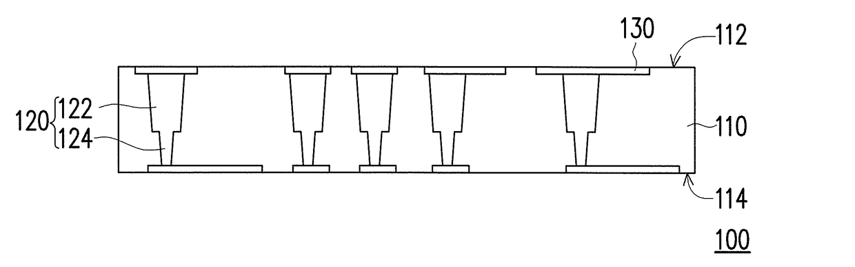
[0032]FIG. 1 is a schematic cross-sectional view of a semiconductor structure according to an embodiment of the invention. Referring to FIG. 1, in the present embodiment, a semiconductor structure 100 includes a first insulating layer 110, a plurality of first stepped conductive vias 120 and a first patterned circuit layer 130. The first insulating layer 110 includes a first top surface 112 and a first bottom surface 114 opposite to the first top surface 112. The first stepped conductive vias 120 are disposed at the first insulating layer 110 to electrically connect the first top surface 112 and the first bottom surface 114. In the present embodiment, the first stepped conductive vias 120 may be formed by laser drilling or laser drilling in combination with mechanical drilling.

[0033]Generally, due to the limitation of the laser process, an aspect ratio of a conductive via formed by laser drilling cannot exceed 3:1. In other words, the depth of each conductive via can only reach, at ...


PUM


Abstract

A semiconductor structure includes an insulating layer, a plurality of stepped conductive vias and a patterned circuit layer. The insulating layer includes a top surface and a bottom surface opposite to the top surface. The stepped conductive vias are disposed at the insulating layer to electrically connect the top surface and the bottom surface. Each of the stepped conductive vias includes a head portion and a neck portion connected to the head portion. The head portion is disposed on the top surface, and an upper surface of the head portion is coplanar with the top surface. A minimum diameter of the head portion is greater than a maximum diameter of the neck portion. The patterned circuit layer is disposed on the top surface and electrically connected to the stepped conductive vias.

Description

CROSS-REFERENCE TO RELATED APPLICATION[0001]This is a continuation-in-part application of and claims the priority benefit of U.S. patent application Ser. No. 15 / 232,808, filed on Aug. 10, 2016, now pending. The prior patent application Ser. No. 15 / 232,808 is continuation-in-part application of patent application Ser. No. 14 / 663,447, filed on Mar. 19, 2015, now issued as U.S. Pat. No. 9,451,694, which claims the priority benefit of Taiwan patent application serial no. 103121829, filed on Jun. 24, 2014. The entirety of each of the above-mentioned patent applications is hereby incorporated by reference herein and made a part of this specification.BACKGROUNDField of the Invention[0002]The invention relates to a semiconductor structure. More particularly, to a semiconductor structure with stepped conductive vias.Description of Related Art[0003]Recently, along with the rapid development of electronic technologies and the semiconductor industry, electronic products that are more user-frien...

Claims


Application Information

Patent Timeline
IPC IPC(8): H01L23/00H01L25/10H01L23/498
CPCH01L23/562H01L23/49827H01L23/49838H01L23/49894H01L23/49822H01L2924/35121H01L24/16H01L25/105H01L2224/16235H01L2225/1058H01L23/49816H05K1/0373H05K1/113H05K1/115H05K3/0014H05K3/105H05K3/188H05K3/4007H05K2201/0236H05K2201/0376H05K2201/09063H05K2201/09118H05K2201/10151H05K2201/10515H05K2201/10674H01L2224/04105H01L2224/12105H01L2224/16227H01L2224/48091H01L2224/48227H01L2225/1023H01L2225/1041H01L2924/18162H01L2924/3511H05K2201/09845H05K3/424H01L2924/15311H01L2924/00014H01L2224/18H01L2224/16225H01L2924/181H01L24/19H01L24/20H01L24/48H01L23/3128H01L2924/00H01L2224/45099H01L2924/00012H05K3/4697H05K2201/0919
Inventor LIU, WEN-CHUNLAI, WEI-JEN
Owner IBIS INNOTECH
Why Eureka
Try Eureka