Methods of Forming Etch Masks for Sub-Resolution Substrate Patterning

a technology of sub-resolution substrates and masks, applied in photomechanical treatment, instruments, electrical equipment, etc., can solve the problems of limiting the pitch or spacing between exposed features, conventional patterning techniques suffer from poor resolution or rough surface of etched features, conventional techniques cannot provide a level of uniformity and fidelity, etc., to achieve the effect of expanding the capabilities of photolithography

Active Publication Date: 2017-03-30
TOKYO ELECTRON LTD
View PDF2 Cites 20 Cited by
  • Summary
  • Abstract
  • Description
  • Claims
  • Application Information

AI Technical Summary

Benefits of technology

[0007]Pitch reduction techniques are termed (often somewhat erroneously yet routinely) “pitch multiplication” as exemplified by “pitch doubling” et cetera. Pitch reduction techniques can extend the capabilities of photolithography beyond feature size limitations (optical resolution limitations). That is, conventional multiplication of pitch (more accurately pitch reduction, or multiplication of pitch density) by a certain factor involves reducing a target pitch by a specified factor. Double patterning techniques used with 193 nm immersion lithography are conventionally considered as one of the most promising techniques to pattern 22 nm nodes and smaller. Noteworthy is that self-aligned spacer double patterning (SADP), or self-aligned quadruple patterning (SAQP), has already been established as a pitch density doubling process and has been adapted in high volume manufacturing of NAND flash memory devices. Moreover, ultra-fine resolution can be obtained to repeat the SADP step twice as pitch quadrupling.

Problems solved by technology

Conventional lithographic techniques for exposing a pattern of radiation or light onto a substrate have various challenges that limit a size of features exposed, and limit pitch or spacing between exposed features.
Although there exist several patterning techniques to increase pattern density or pitch density, conventional patterning techniques suffer from poor resolution or rough surfaces of etched features.
Thus, conventional techniques cannot provide a level of uniformity and fidelity desired for very small dimensions (20 nm and smaller).
Moreover, with pitch density doubling and quadrupling techniques, sub-resolution lines can be created, but making cuts or connections between these lines is challenging, especially since the pitch and dimensions needed for such cuts is far below capabilities of conventional photo-lithography systems.

Method used


Image

  • Methods of Forming Etch Masks for Sub-Resolution Substrate Patterning
  • Methods of Forming Etch Masks for Sub-Resolution Substrate Patterning
  • Methods of Forming Etch Masks for Sub-Resolution Substrate Patterning

Examples


Embodiment Construction

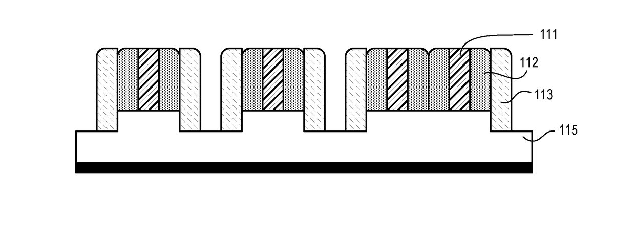
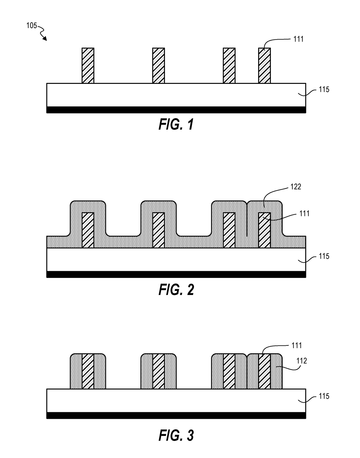
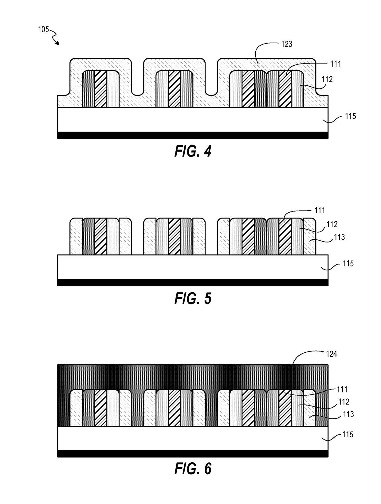
[0019]Techniques disclosed herein, provide a method and fabrication structure for pitch reduction (increasing pitch / feature density) for creating high-resolution features and also for cutting on pitch of sub-resolution features. Techniques include using multiple materials having different etch characteristics to selectively etch features and create cuts or blocks where specified. This can include creating a repeating pattern of materials having a pattern of A-B-C-D-C-B-A, with half pitches below 40 nanometers and even below 12 nanometers and smaller. Critical dimensions of materials can be controlled by type of deposition thickness, such as with atomic layer deposition, instead of being controlled just by optical resolution.

[0020]One embodiment includes a method of patterning a substrate. Such a method is useful for microfabrication of semiconductor devices and integrated circuits. Referring now to FIG. 1, the method includes providing a substrate 105 having mandrels 111 positioned ...


PUM


Abstract

Techniques disclosed herein provide a method for pitch reduction (increasing pitch / feature density) for creating high-resolution features and also for cutting on pitch of sub-resolution features. Techniques include using multiple materials having different etch characteristics to selectively etch features and create cuts where specified. A sequence of materials or repeating pattern of lines of materials is used that provides selective self-alignment based on different etch resistivities. Combined with an underlying transfer or memorization layer, multiple different etch selectivities can be accessed. An etch mask defines which regions of the lines of multiple materials can be etched.

Description

CROSS REFERENCE TO RELATED APPLICATIONS[0001]The present application claims the benefit of U.S. Provisional Patent Application No. 62 / 232,005, filed on Sep. 24, 2015, entitled “Methods of Forming Etch Masks for Sub-Resolution Substrate Patterning,” which is incorporated herein by reference in its entirety. The present application also claims the benefit of U.S. Provisional Patent Application No. 62 / 258,119, filed on Nov. 20, 2015, entitled “Methods of Forming Etch Masks for Sub-Resolution Substrate Patterning,” which is incorporated herein by reference in its entirety.BACKGROUND OF THE INVENTION[0002]This disclosure relates to substrate processing, and, more particularly, to techniques for patterning substrates including patterning semiconductor wafers.[0003]Methods of shrinking line-widths in lithographic processes have historically involved using greater-NA optics (numerical aperture), shorter exposure wavelengths, or interfacial media other than air (e.g., water immersion). As th...

Claims


Application Information

Patent Timeline
Patent Type & Authority Applications(United States)
IPC IPC(8): H01L21/033H01L21/311H01L21/308
CPCH01L21/0337H01L21/31144H01L21/3086H01L21/0274G03F7/0002H01L21/31056H01L21/3081
Inventor DEVILLIERS, ANTON J.
Owner TOKYO ELECTRON LTD
Why Eureka
Try Eureka