

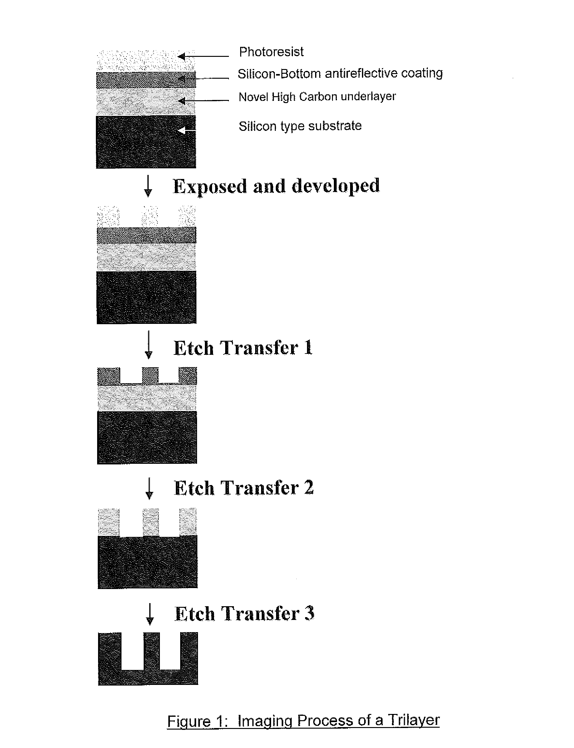
Antireflective coating compositions and processes thereof
a technology of coating composition and composition, applied in the direction of photomechanical treatment originals, instruments, photomechanical equipment, etc., can solve the problems of back reflectivity, thin film interference effect and reflective notching, and change in critical line width dimensions
- Summary
- Abstract
- Description
- Claims
- Application Information
AI Technical Summary
Benefits of technology
Problems solved by technology
Method used
Image


Examples
process example 1a
Solvent Resistance of Formulation 1a
[0078]Formulation 1a was spin-coated on an 8″ silicon wafer and baked at 450° C. for 60 sec resulting in a 400 nm thick film. This film was treated with PGMEA for 10 sec and showed no significant thickness loss. This showed that a crosslinker is not essential to impart insolubility.
process example 1b
Elemental Analysis of Formulation 1b
[0079]Formulation 1 b was spin-coated on an 8″ silicon wafer and baked at 230° C. for 60 sec. The coated material was scraped out from the wafer surface by a blade and elemental analysis was done. In the same way, Formulation 1b baked at 400° C. for 120 sec and elemental analysis was done. The results are shown in the Table 1. Also, the film spun and baked as described above at 2 different temperatures, did not show any significant thickness loss when treated with PGMEA for 10 sec.
TABLE 1Formulation 1bC (%)H (%)O (%)Baked at 230° C. for 60 sec86.224.679.11Baked at 400° C. for 120 sec83.033.8413.13
Formulation 2
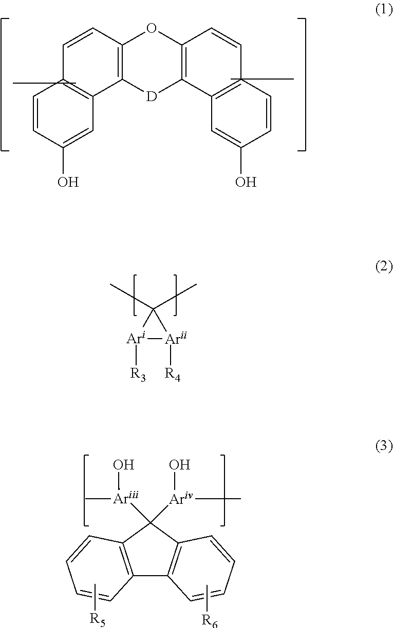
[0080]A solution was prepared by mixing Polymer 1 (2.6316 g), 3,3′,5,5′-tetrakis(methoxymethyl)-[(1,1′-biphenyl)-4,4′-diol] (0.2632 g), a 10 wt % PGMEA solution of triethylammonium dodecylbenzenesulfonate (1.0536 g) and 26.0526 g of PGMEA. After complete mixing, the solution was filtered through a 0.02 μm filter and used for via filling exper...
process example 2
with Formulation 2
[0081]Via filling of Formulation 2 was tested as described above. SEM cross sections showed that 100 nmVias (pitches 1000 nm, 250 nm and 200 nm) were completely filled with the Formulation 2, and no visible pinholes, voids or other defects was observed.
Formulation 3
[0082]A solution was prepared by mixing Polymer 1 (2.6316 g), 3,3′,5,5′-tetrakis(methoxymethyl)-[(1,1′-biphenyl)-4,4′-diol] (0.2632 g), a 10 wt % PGMEA solution of triethylammonium dodecylbenzenesulfonate (1.0536 g) and 26.0526 g of PGMEA. After complete mixing, the solution was filtered through a 0.02 μm filter and used for outgassing experiment.
PUM
| Property | Measurement | Unit |
|---|---|---|
| Temperature | aaaaa | aaaaa |
| Temperature | aaaaa | aaaaa |
| Temperature | aaaaa | aaaaa |
Abstract
Description
Claims
Application Information