Group iii nitride semiconductor light-emitting device

a semiconductor and light-emitting technology, applied in the direction of semiconductor devices, basic electric elements, electrical apparatus, etc., can solve the problems of uneven distribution of electrons in the light-emitting layer thickness direction, inability to consider the density of electrons injected into the light-emitting layer, and inability to achieve uniform thickness of electrons, so as to achieve the effect of increasing the number of electrons contributing to light-emitting, high energy level of electrons injected into the activ

Active Publication Date: 2017-03-30
TOYODA GOSEI CO LTD
View PDF2 Cites 12 Cited by
  • Summary
  • Abstract
  • Description
  • Claims
  • Application Information

AI Technical Summary

Benefits of technology

[0029]In the present invention, an electron injection adjusting layer comprising a single layer made of AlxGayIn1-x-yN (0<x<1, 0<y<1, 0<x+y≦1) is formed in the base layer or as its top layer. The electron injection adjusting layer has the highest electron level of the bottom of conduction band in the base layer and the n-type superlattice layer, that is, in the n-type layers up to the light-emitting layer. Therefore, the electron injection adjusting layer provides a potential barrier against electrons to be injected into the active layer. As a result, the energy level of the electrons injected into the active layer is high, and the diffusion length of the e

Problems solved by technology

However, the electron density is highest at an interface between the light-emitting layer and the p-type cladding layer due to long diffusion length of the electrons, and a region having a high electron density is formed near the interface so that the electrons are not uniformly distributed in a thickness direction of the light-emitting layer.
As a result, there a

Method used


Image

  • Group iii nitride semiconductor light-emitting device
  • Group iii nitride semiconductor light-emitting device
  • Group iii nitride semiconductor light-emitting device

Examples


embodiment 1

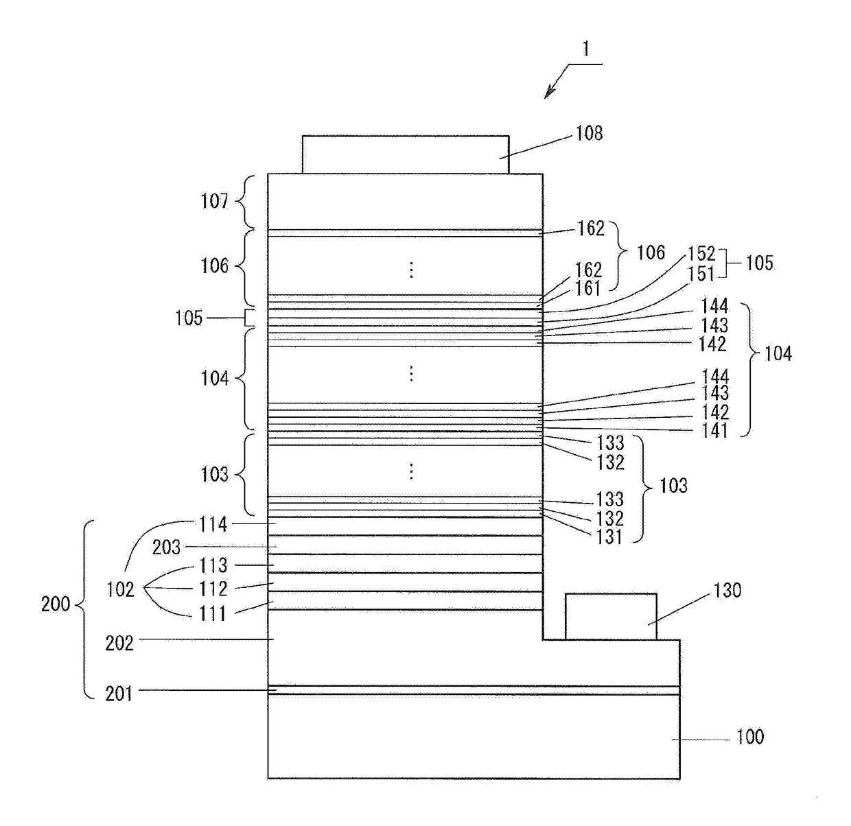
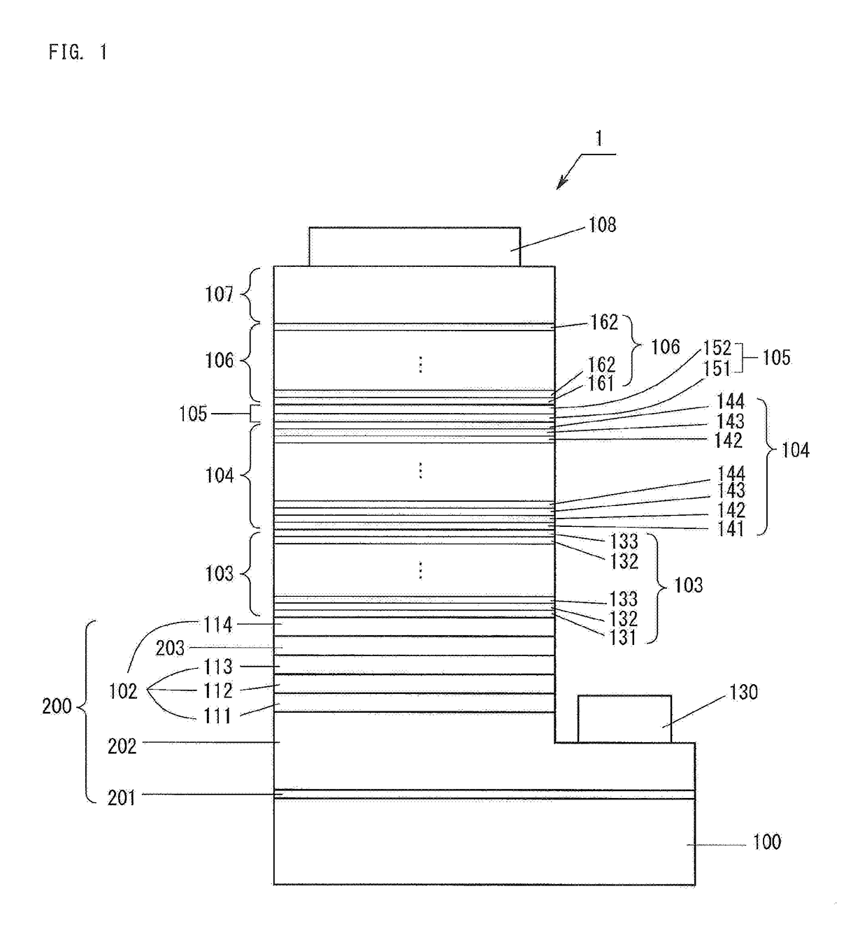
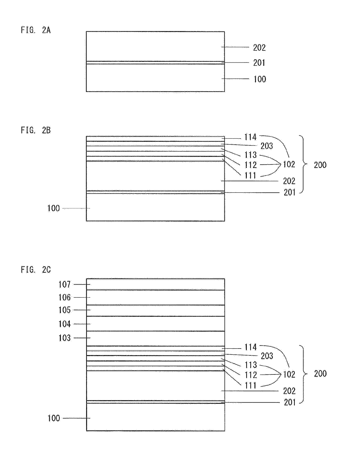
[0035]FIG. 1 shows the structure of a light-emitting device 1 according to Embodiment 1. The light-emitting device 1 has a structure a sapphire substrate 100; an n-type contact layer 202, an ESD layer (a layer for improving electrostatic breakdown voltage) 102, an n-type layer side superlattice layer (hereinafter, referred to as “n-type superlattice layer”) 103, a light-emitting layer 104, an undoped cladding layer 105, a p-type layer side cladding layer (hereinafter, referred to as “p-type cladding layer”) 106, and a p-type contact layer 107, the layers 202 to 107 being formed of a Group III nitride semiconductor and deposited on the substrate 100 via an AlN buffer layer 201; a p-electrode 108 formed on the p-type contact layer 107; and an n-electrode 130 formed on a portion of the n-type contact layer 202 exposed through removal of the corresponding portions of the layers 102 to 107 by etching from the p-type contact layer 107. A base layer 200 is a stack of all the single crystal...


PUM


Abstract

The present invention provides a Group III nitride semiconductor light-emitting device exhibiting improved emission efficiency. The Group III nitride semiconductor light-emitting device includes a base layer, an n-type superlattice layer, a light-emitting layer, and a p-type cladding layer, each of the layers being made of Group III nitride semiconductor. An electron injection adjusting layer comprising a single AlxGa1-xN (0<x<1) layer and having a thickness of 5 Å to 30 Å is formed in the base layer. The n-type superlattice layer is a superlattice layer having a periodic structure of an InyGa1-yN (0<y<1) layer, an i-GaN layer, and an n-GaN layer. The electron injection adjusting layer has a thickness of 5 Å to 30 Å and an Al composition ratio of 0.15 to 0.5.

Description

BACKGROUND OF THE INVENTION[0001]Field of the Invention[0002]The present invention relates to a Group III nitride semiconductor light-emitting device exhibiting improved emission efficiency.[0003]Background Art[0004]A Group III nitride semiconductor light-emitting device such as high brightness blue LED has been put into practical use. The light-emitting device has a double hetero structure in which a light-emitting layer having a MQW structure is sandwiched between an n-type cladding layer and a p-type cladding layer. Holes injected from the p-type cladding layer to the light-emitting layer hardly overflow from the n-type cladding layer because the holes are effectively confined in the light-emitting layer having a MQW structure due to a short diffusion length. Therefore, there is no need to form a potential barrier layer for the holes in the valence band as the function of the n-type cladding layer.[0005]The inventors of the present invention came up with an idea that a strain rel...

Claims


Application Information

Patent Timeline
IPC IPC(8): H01L33/14H01L33/32H01L33/04H01L33/00H01L33/44
CPCH01L33/14H01L33/0075H01L33/0025H01L33/04H01L33/32H01L33/44
Inventor OKUNO, KOJI
Owner TOYODA GOSEI CO LTD
Why Eureka
Try Eureka