Semiconductor devices and inverter having the same

a technology of semiconductor devices and inverters, which is applied in the direction of semiconductor devices, pulse techniques, logic circuits, etc., can solve the problems of deteriorating gate channel characteristics, significantly decreasing the alternative current (ac) performance of cmos devices, and deteriorating parasitic capacitance and electrical resistance, so as to improve the operation increase the ac performance of cmos inverters. , the effect of contact resistance between the boundary gate structur

a technology of semiconductor devices and inverters, which is applied in the direction of semiconductor devices, pulse techniques, logic circuits, etc., can solve the problems of deteriorating gate channel characteristics, significantly decreasing the alternative current (ac) performance of cmos devices, and deteriorating parasitic capacitance and electrical resistance, so as to improve the operation increase the ac performance of cmos inverters. , the effect of contact resistance between the boundary gate structur

US20170103986A1Active Publication Date: 2017-04-13SAMSUNG ELECTRONICS CO LTD

Image

  • Semiconductor devices and inverter having the same
  • Semiconductor devices and inverter having the same
  • Semiconductor devices and inverter having the same

Examples


Embodiment Construction

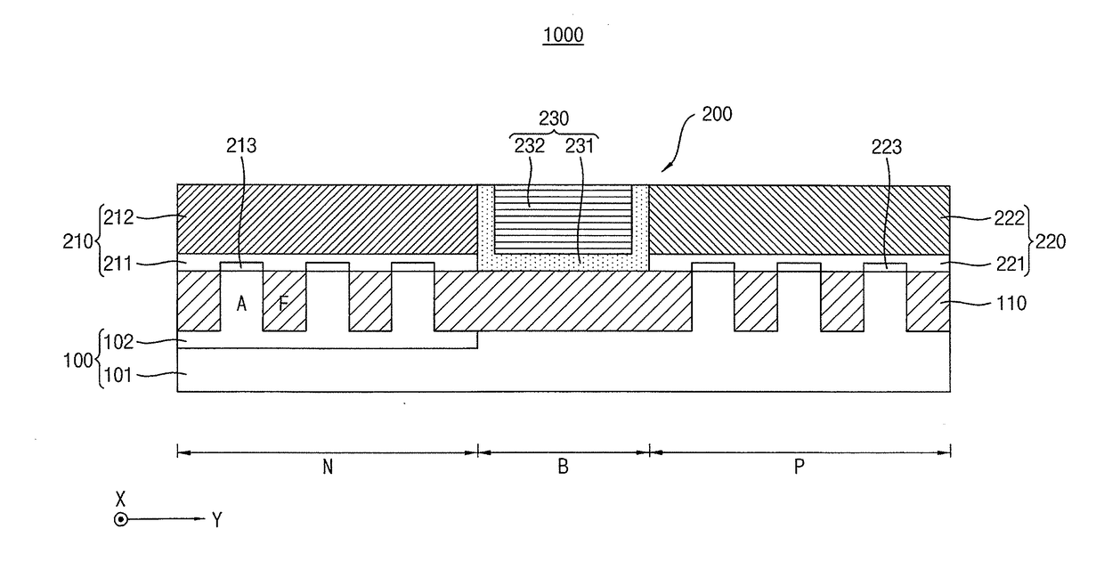
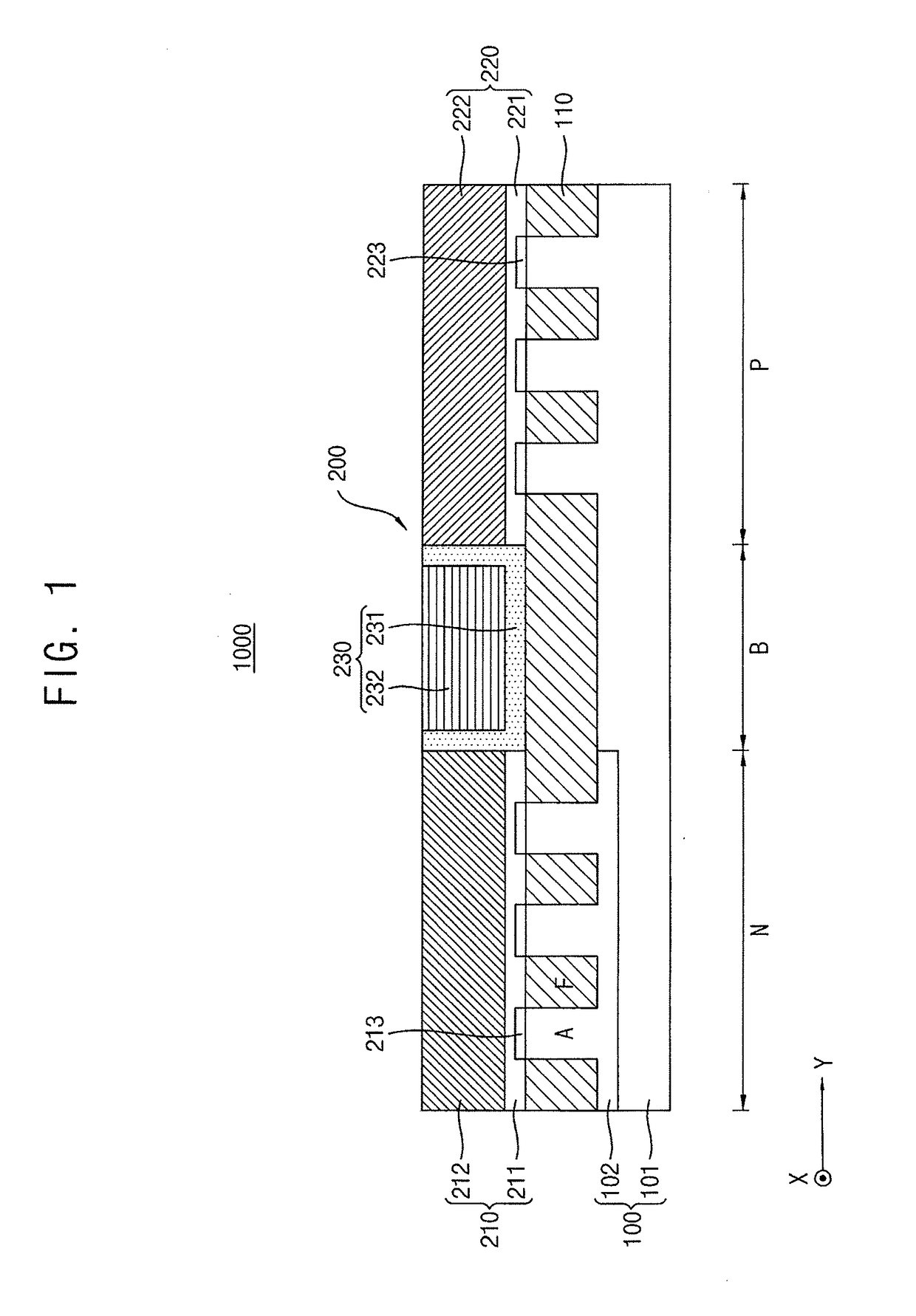
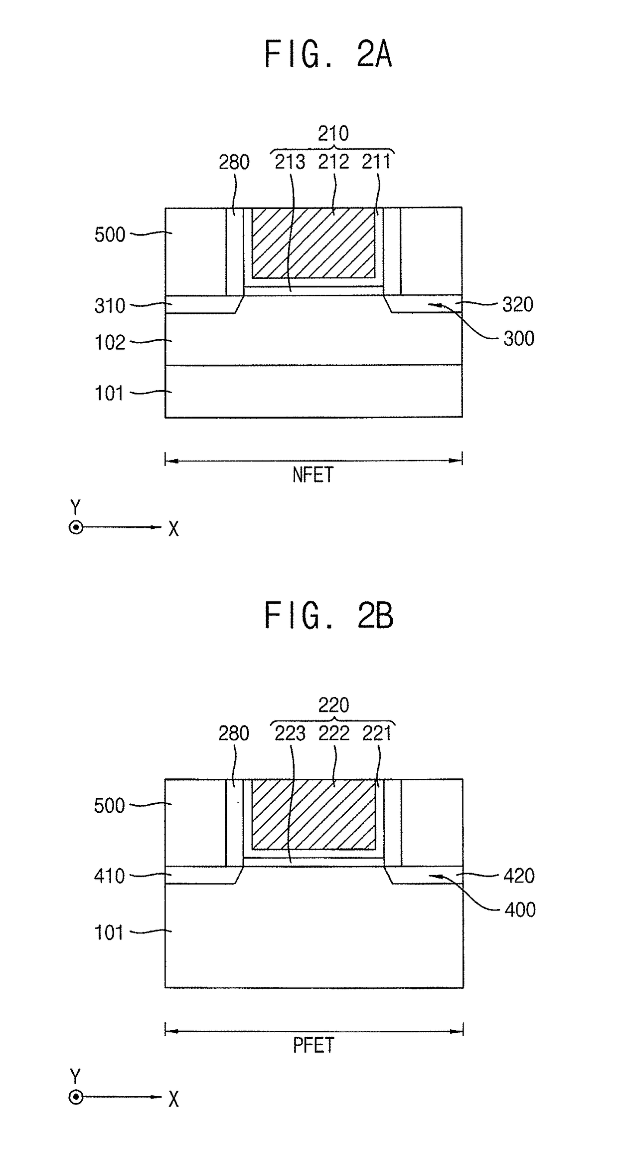
[0051]Various example embodiments will be described more fully hereinafter with reference to the accompanying drawings, in which some example embodiments are shown. The present inventive concept may, however, be embodied in many different forms and should not be construed as limited to the specific example embodiments set forth herein. Rather, these example embodiments are provided so that this description will be thorough and complete, and will fully convey the scope of the present inventive concept to those skilled in the art.

[0052]It will be understood that when an element or layer is referred to as being “on”, “connected to” or “coupled to” another element or layer, it can be directly on, connected or coupled to the other element or layer, or intervening elements or layers may be present. In contrast, when an element is referred to as being “directly on”, “directly connected to” or “directly coupled to” another element or layer, there are no intervening elements or layers presen...


PUM


Abstract

Disclosed are CMOS device and CMOS inverter. The CMOS device includes a substrate having active lines extending in a first direction and defined by a device isolation layer, the substrate being divided into an NMOS area, a PMOS area and a boundary area interposed between the NMOPS and the PMOS areas and having the device isolation layer without the active line, a gate line extending in a second direction across the active lines and having a first gate structure on the active line in the first area, a second gate structure on the active line in the second and a third gate structure on the device isolation layer in the third area. The electrical resistance and parasitic capacitance of the third gate structure are smaller than those of the NMOS and the PMOS gate structures. Accordingly, better AC and DC performance of the CMOS device can be obtained.

Description

CROSS-REFERENCE TO RELATED APPLICATIONS[0001]This application claims priority under 35 U.S.C §119 to Korean Patent Application No. 10-2015-0141584 filed on Oct. 8, 2015 in the Korean Intellectual Property Office, the contents of which are incorporated by reference herein in their entirety.TECHNICAL FIELD[0002]The present invention generally relates to a semiconductor device and an inverter having the same, and more particularly, to a complementary metal oxide semiconductor (CMOS) device having a p-type MOS (PMOS) device and an n-type MOS (NMOS) device, and a CMOS inverter having the CMOS.DISCUSSION OF RELATED ART[0003]As the recent memory devices being highly integrated and miniaturized, the size of the active regions in the semiconductor substrate may be reduced. The reduction of the gate width and the channel length in the cell transistors may cause the gate resistance and the threshold voltage to increase. Particularly, the decrease of the channel length in the metal oxide semico...

Claims


Application Information

Patent Timeline
13 Apr 2017
Publication
US20170103986A1
IPC
H01L27/092
CPC
H01L27/0924; H01L29/51; H01L29/49; H01L27/088; H01L29/42356; H03K19/018507; H01L21/823821; H01L21/823828
Inventors
KIM, MUN-HYEON; NOH, CHANG-WOO