Three Terminal Spin Orbit Torque Memory Cell with In-Stack MAGNETIC LAYER THAT PROVIDES Magnetic Bias Field AND SPIN ORBIT TORQUE VIA Anomalous Hall Effect

a memory cell and spin orbit technology, applied in the field of memory cells in a random access memory device (mram), can solve the problems of neighboring cells being erroneously written, scalding these devices to high densities, and the current required to generate sufficient field to switch the free layer becomes prohibitively larg

Active Publication Date: 2017-05-04
WESTERN DIGITAL TECH INC
View PDF0 Cites 67 Cited by
  • Summary
  • Abstract
  • Description
  • Claims
  • Application Information

AI Technical Summary

Benefits of technology

[0009]In one embodiment, an SOT-MRAM memory cell is provided. The SOT-MRAM memory cell includes a free layer, a non-magnetic spin orbit torque (SOT) layer, an exchange-pinned ferromagnetic bias layer, and an antiferromagnetic (AFM) layer. The SOT layer is chosen to exhibit a substantial spin-Hall effect (SHE). It is positioned below the free layer, and is configured to provide spin orbit torque on the free layer via SHE when electrical (write) current is passed through it. The ferromagnetic bias layer is positioned below the SOT (or SHE) layer and is configured to provide a static in-plane magnetic bias field to the free magnetic layer to achieve deterministic switching of the free layer from a first magnetization state to a second magnetization state. The AFM layer is positioned below the ferromagnetic bias layer. The AFM layer is configured to exchange pin a preferred magnetization direction of the ferromagnetic bias layer.
[0010]In another embodiment, a SOT-MRAM memory cell is disclosed herein. The SOT-MRAM memory cell includes a free layer, a nonmagnetic spacer layer, an exchange pinned ferromagnetic bias layer and an AFM layer. In this case, the ferromagnetic bias layer is chosen to produce a substantial anomalous Hall effect (AHE) to provide spin orbit torque on the free layer, in addition to also providing a static in-plane magnetic bias field to permit a deterministic switching of the free layer from a first magnetization state to a second magnetization state. The spacer is positioned between the free layer and the magnetic bias / AHE layer. The spacer magnetically decouples the free layer from the bias layer, and allows passage of a spin current from the magnetic bias / AHE layer to the free layer when an electrical (write) current flows in the bias / AHE layer. The AFM layer is positioned below the magnetic bias layer. The AFM layer is configured to exchange pin a preferred magnetization direction of the ferromagnetic bias layer.
[0011]In another embodiment, a method for deterministically switching a free layer in an SOT-MRAM cell is disclosed herein. The method includes providing a current through a spin Hall effect layer such that a magnetization direction of a ferromagnetic bias layer creates an angle with respect to a direction of the current to generate a magnetic bias field parallel with the direction of the current as well as a spin current perpendicular to the cell to deterministically switch a free layer from a first magnetization state to a second magnetization state.

Problems solved by technology

Significant problems arise when scaling these devices to high densities.
Particularly, the currents required to generate sufficient field to switch the free layer become prohibitively large, and disturbances to neighboring cells or elements can occur during writing, which in turn may cause a neighboring cell to be erroneously written.

Method used


Image

  • Three Terminal Spin Orbit Torque Memory Cell with In-Stack MAGNETIC LAYER THAT PROVIDES Magnetic Bias Field AND SPIN ORBIT TORQUE VIA Anomalous Hall Effect
  • Three Terminal Spin Orbit Torque Memory Cell with In-Stack MAGNETIC LAYER THAT PROVIDES Magnetic Bias Field AND SPIN ORBIT TORQUE VIA Anomalous Hall Effect
  • Three Terminal Spin Orbit Torque Memory Cell with In-Stack MAGNETIC LAYER THAT PROVIDES Magnetic Bias Field AND SPIN ORBIT TORQUE VIA Anomalous Hall Effect

Examples


Embodiment Construction

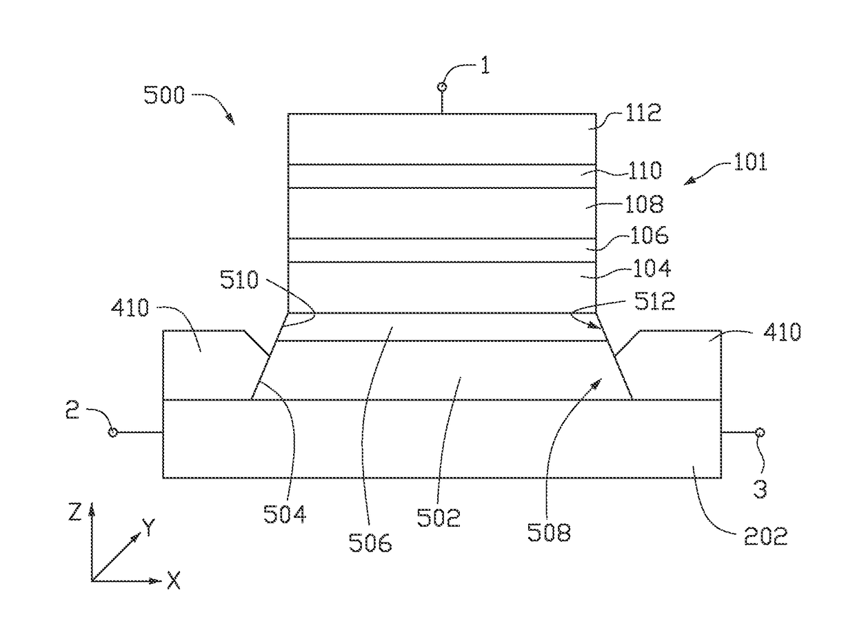
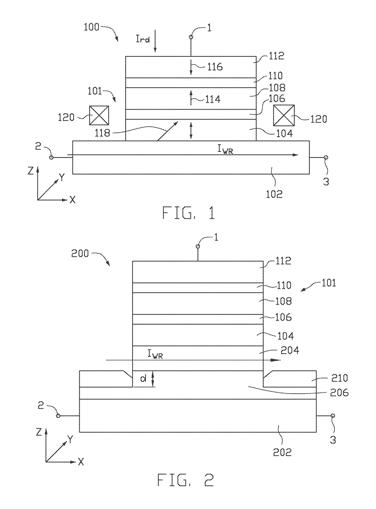
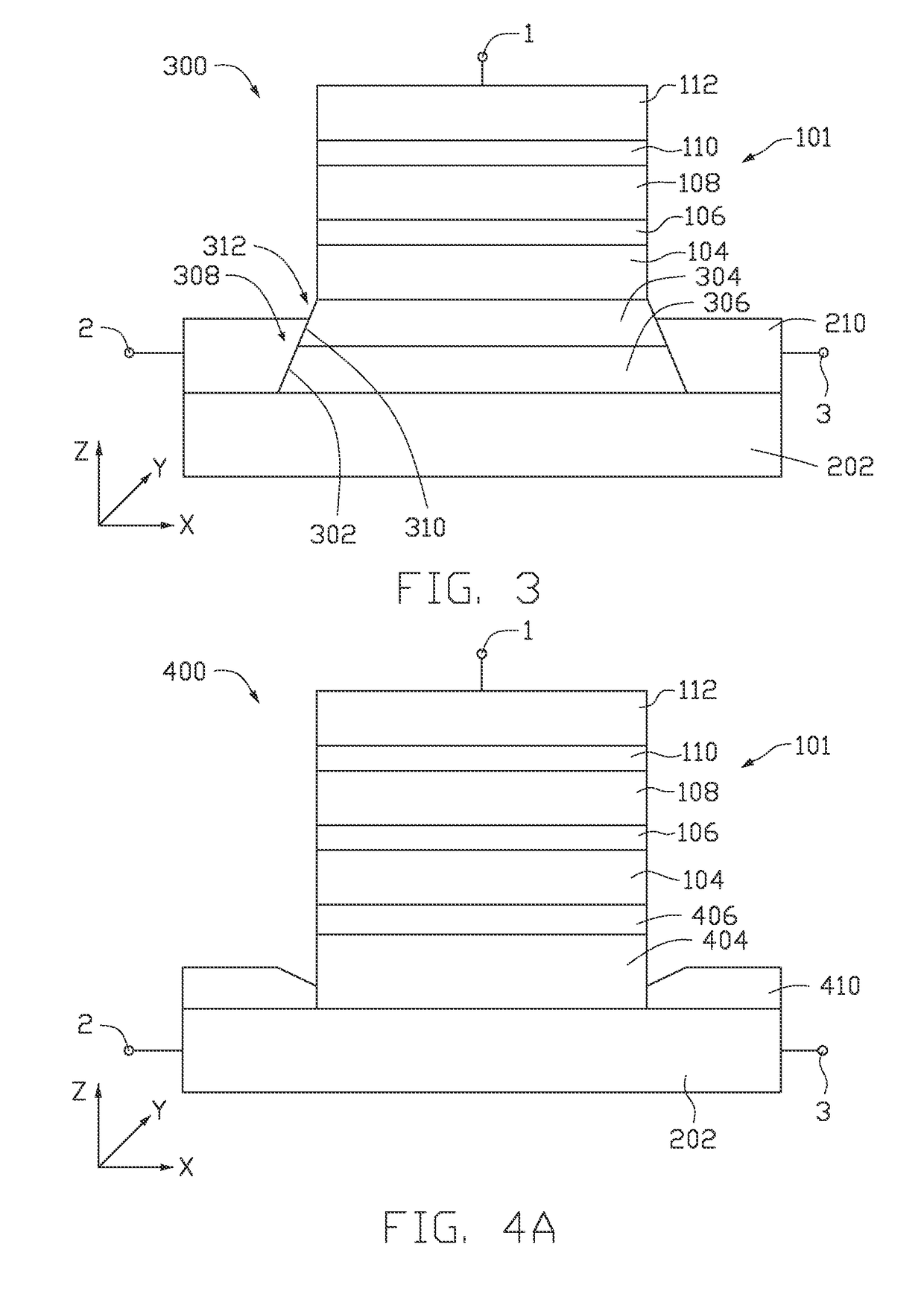
[0021]In the following, reference is made to embodiments of the disclosure. However, it should be understood that the disclosure is not limited to specific described embodiments. Instead, any combination of the following features and elements, whether related to different embodiments or not, is contemplated to implement and practice the disclosure. Furthermore, although embodiments of the disclosure may achieve advantages over other possible solutions and / or over the prior art, whether or not a particular advantage is achieved by a given embodiment is not limiting of the disclosure. Thus, the following aspects, features, embodiments, and advantages are merely illustrative and are not considered elements or limitations of the appended claims except where explicitly recited in a claim(s). Likewise, reference to “the disclosure” shall not be construed as a generalization of any inventive subject matter disclosed herein and shall not be considered an element or limitation of the appende...


PUM


Abstract

A method and apparatus for deterministically switching a free layer in a spin orbit torque magnetoresistive random access memory (SOT-MRAM) cell is disclosed herein. In one embodiment, an SOT-MRAM memory cell is provided. The SOT-MRAM memory cell includes a magnetic tunnel junction, a ferromagnetic bias layer, and an antiferromagnetic layer. The magnetic tunnel junction includes a free layer having primarily two bi-stable magnetization directions, a reference layer having a fixed magnetization direction, and an insulating tunnel barrier layer positioned between the free layer and the reference layer. The ferromagnetic bias layer is configured to provide spin orbit torque via anomalous Hall effect and simultaneously configured to provide a magnetic bias field on the free layer to achieve deterministic switching. The antiferromagnetic layer is positioned below the ferromagnetic bias layer and is configured to pin a magnetization direction of the ferromagnetic bias layer in a predetermined direction.

Description

BACKGROUND OF THE DISCLOSURE[0001]Field of the Disclosure[0002]Embodiments of the present disclosure generally relate to magnetic storage elements, and more particularly to memory cells in a magnetoresistive random-access memory device (MRAM).[0003]Description of the Related Art[0004]MRAM is a non-volatile random-access memory technology. Unlike conventional RAM, data in MRAM devices are not stored as electric charge or current flows. Rather, data is stored by magnetic storage elements. MRAM devices include cells or elements having a magnetically hard layer (i.e., a “reference” layer) and a magnetically soft layer (i.e., the “free” layer). Writing to MRAM is performed by passing current through current leads that are formed on either side of each memory element in order to create a local induced magnetic field, which sets the direction of the soft layer magnetization. Significant problems arise when scaling these devices to high densities. Particularly, the currents required to gene...

Claims


Application Information

Patent Timeline
Patent Type & Authority Applications(United States)
IPC IPC(8): G11C11/16H01L43/10H01L43/04H01L43/08H01L43/06
CPCG11C11/161H01L43/08G11C11/1675H01L43/04H01L43/10H01L43/065G11C11/1659G11C11/18H10N50/10H10N50/85H10N52/80H10N52/101
Inventor MIHAJLOVIC, GORANSMITH, NEIL
Owner WESTERN DIGITAL TECH INC
Why Eureka
Try Eureka