Process for producing glass substrate and glass substrate

a technology of glass substrate and glass substrate, which is applied in the direction of glass rolling apparatus, glass tempering apparatus, instruments, etc., can solve the problems of not maintaining electric properties, difficult to reduce the thickness of glass substrate, and inability to dispose of a long annealing furnace like in the float method, etc., to achieve the effect of increasing the cost of polishing, and increasing the size of glass substra

Active Publication Date: 2009-09-10
NIPPON ELECTRIC GLASS CO LTD
View PDF11 Cites 66 Cited by
  • Summary
  • Abstract
  • Description
  • Claims
  • Application Information

AI Technical Summary

Benefits of technology

[0052]According to this constitution, the effect of the invention is more remarkable. Specifically, as a heat treatment method which does not require polishing, known is the method in the above-mentioned Patent Reference 1 where substrates are stood vertically in heat treatment thereof. However, when the substrates are more large-sized, then the glass may be readily distorted or warped in the method in Patent Reference 1. On the other hand, in the invention, even when the substrate size is large, it produces no disadvantages accompanied by the distortion or warpage.
[0053]According to this constitution, the effect of the process of the invention is more remarkable. Specifically, ordinary off-line annealing requires polishing, in which, therefore, when the substrate is larger, then the polishing cost increases or the polishing itself may be difficult. Even in the method of Patent Reference 1 which does not require polishing, distortion or warpage tends to occur when the size of the glass substrate is large. Accordingly, the larger the size of the glass substrate is, the larger the advantage of the glass substrate of the invention is.
[0054]Preferably, the glass substrate of the invention is for use in a flat panel display.
[0055]According to this constitution, since the substrate hardly shrinks and circuit pattern deviation hardly occurs in the heat treatment in a production step for a flat panel display, the substrate can be used in a display with a low-temperature p-SiTFT mounted thereon.
[0056]For the substrate of the invention, the flat panel display is preferably a display in which a low-temperature p-SiTFT is formed on the substrate.
[0057]According to the constitution, the substrate hardly shrinks even when exposed to high-temperature condition in forming a low-temperature p-SiTFT thereon. Accordingly, the circuit pattern to be formed on the substrate is prevented from being deviated from the originally planned one and therefore the drawback thereof to lose the electric properties can be effectively evaded.ADVANTAGE OF THE INVENTION

Problems solved by technology

When the thermal shrinkage is large, then the circuit pattern formed on the glass substrate may deviate from the initially planned one, thereby having a fatal defect in that it could not maintain electric properties.
However, the float method has some disadvantages in that it is difficult to reduce the thickness of the glass substrate and, in addition, the glass substrate must be polished to remove the tin adhering to the glass surface.
However, in the down draw method, an annealing furnace is provided just below the forming body, and therefore it is in fact impossible to dispose a long annealing furnace like in the float method.
Accordingly, the annealing furnace is necessarily short, or that is, the cooling rate in the annealing furnace is high and a glass is solidified in a rapidly-cooled state, and therefore the method is problematic in that a glass substrate having a small thermal shrinkage could not be obtained.

Method used


Image

  • Process for producing glass substrate and glass substrate
  • Process for producing glass substrate and glass substrate
  • Process for producing glass substrate and glass substrate

Examples


examples

[0138]Examples and Comparative Examples of the invention are described in detail hereinunder, with reference to the drawings attached hereto.

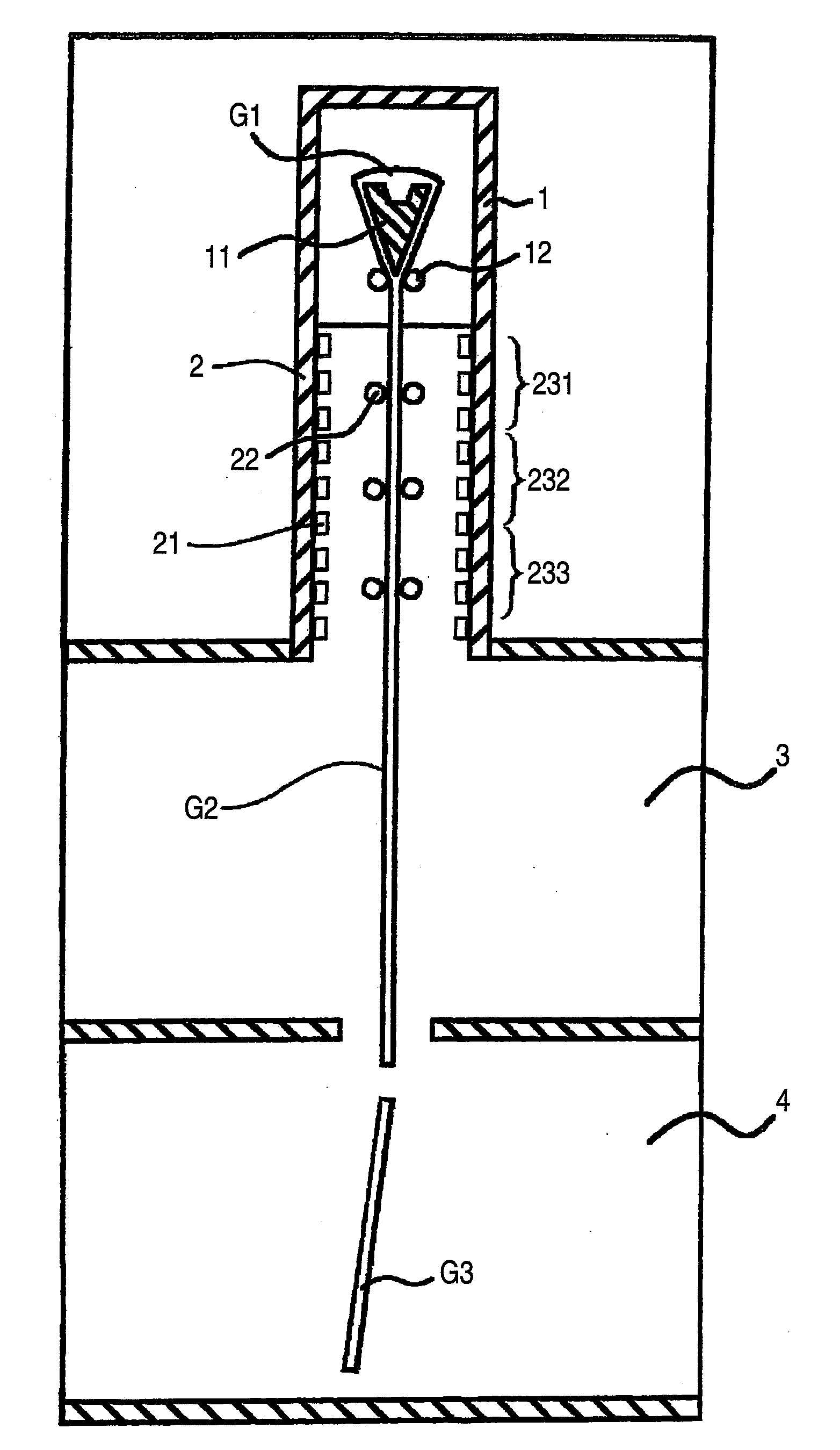
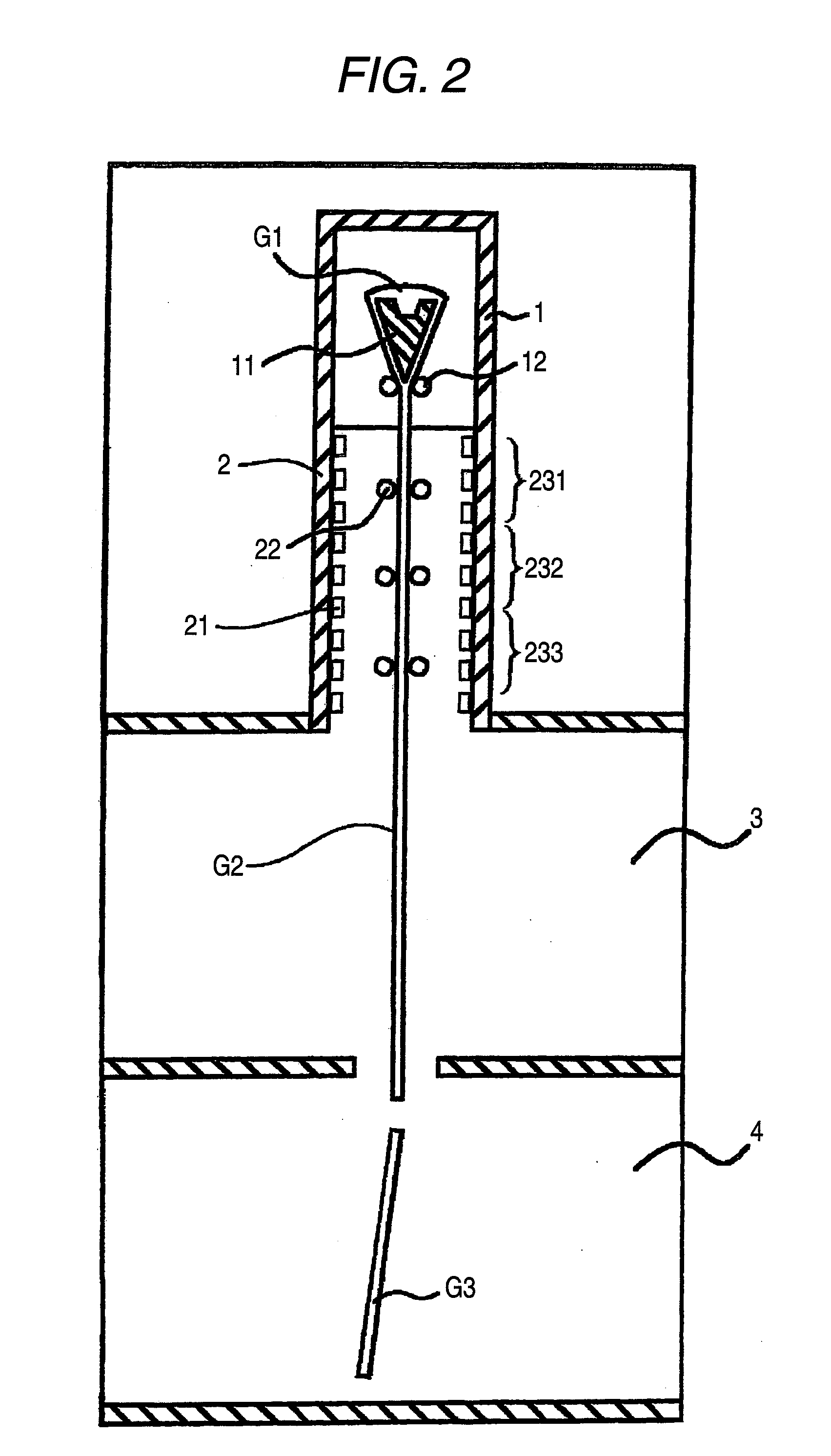
[0139]FIG. 2 is an outline front view showing a production apparatus for a glass substrate in carrying out the invention. The production apparatus is for producing a glass substrate according to an overflow down draw method, and includes a forming furnace 1 in which a molten glass G1 fed to the funnel-like forming body 11 having a nearly wedge-shaped cross section is made to overflow out from the top thereof and is fused at the bottom thereof to form a glass ribbon G3, an annealing furnace 2 in which the glass ribbon G2 is annealed to reduce the thermal shrinkage thereof, a cooling chamber 3 in which the annealed glass ribbon G2 is fully cooled, and a cutting chamber 4 in which the cooled glass ribbon G2 is cut into a predetermined size, each disposed in that order from the top thereof. In this Example, the overall length of the annealing furna...


PUM

PropertyMeasurementUnit
temperatureaaaaaaaaaa
widthaaaaaaaaaa
liquidus viscosityaaaaaaaaaa

Abstract

Provided are a process for producing a glass substrate usable for low-temperature p-SiTFT substrates directly in accordance with a down draw method, and the glass substrate obtained by the process. The process for producing a glass substrate includes a forming step of forming a molten glass into a ribbon shape in accordance with a down draw method, an annealing step of annealing the glass ribbon, and a cutting step of cutting the glass ribbon to give a glass substrate, in which, in the annealing step, an average cooling rate from the annealing point to the (annealing point −50° C.) is lower than an average cooling rate from the (annealing point +100° C.) to the annealing point.

Description

TECHNICAL FIELD[0001]The present invention relates to a process for producing a glass substrate and a glass substrate, in particular to a glass substrate suitable for so-called a low-temperature p-SiTFT-type display to be driven by a polycrystalline silicon-type thin-film transistor device.BACKGROUND ART[0002]As a substrate for flat panel displays such as liquid-crystal displays, an aluminosilicate-type glass substrate has been widely used. The glass substrate for use in this application is required to have a small thermal shrinkage. Specifically, since a thin-film electric circuit is formed on the glass substrate, the glass substrate undergoes film formation heat treatment, patterning and the like treatment, and in these treatments, the glass substrate is exposed to a high temperature. At that time, structural relaxation occurs, and its volume thereby shrinks. When the thermal shrinkage is large, then the circuit pattern formed on the glass substrate may deviate from the initially ...

Claims


Application Information

Patent Timeline
Patent Type & Authority Applications(United States)
IPC IPC(8): B32B17/00C03B17/06C03B21/02
CPCC03B17/067C03B25/025Y10T428/24355G02F2001/133302C03C3/091G02F1/133302Y02P40/57
Inventor KATO, YOSHINARIMATSUKI, EIJI
Owner NIPPON ELECTRIC GLASS CO LTD
Why Eureka
Try Eureka