
System and method for application specific integrated circuit design

a technology of integrated circuits and design methods, applied in the field of application specific integrated circuit design, can solve the problems of requiring significant manual intervention, most laborious and time-consuming aspects of conventional clock tree synthesis and timing closure, and high risk of systemic and random variation in the distribution of clock signals, so as to simplify the floor plan and simplify the synthesis of clock tree and routing.

Active Publication Date: 2017-05-18
CHRONOS TECH LLC
View PDF2 Cites 5 Cited by
  • Summary
  • Abstract
  • Description
  • Claims
  • Application Information

AI Technical Summary

Benefits of technology

The patent describes a method for designing application-specific integrated circuits using a protocol called Chronos Links. This protocol allows different blocks of the circuit to communicate with each other using messages and signals. The method involves replacing traditional links with Chronos Links, simplifying the layout of the circuit, and optimizing the timing of the circuit. The technical effects of the patent are improved communication between different parts of the circuit and more efficient use of space and resources.

Problems solved by technology

In fact, timing closure for a clock signal that is distributed over a large and complex ASIC design typically requires the strategic placement of numerous buffers.
Moreover, the distribution of a clock signal is also highly susceptible to both systematic and random variations.
As such, the most laborious and time consuming aspects of conventional ASIC design tends to be clock alignment and timing closure.
Clock tree synthesis and timing closure generally require significant manual intervention.
In addition, the mechanisms (i.e., buffers) used to balance the clock across an ASIC chip generally consume a majority of the power in any conventional ASIC design.

Method used


Image

  • System and method for application specific integrated circuit design
  • System and method for application specific integrated circuit design
  • System and method for application specific integrated circuit design

Examples


Embodiment Construction

[0021]While certain embodiments are described, these embodiments are presented by way of example only, and are not intended to limit the scope of protection. The methods and systems described herein may be embodied in a variety of other forms. Furthermore, various omissions, substitutions, and changes in the form of the example methods and systems described herein may be made without departing from the scope of protection.

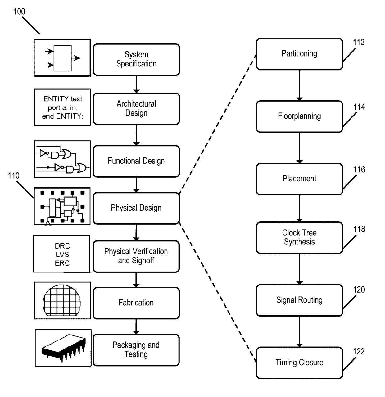
[0022]FIG. 1 is a flowchart illustrating a conventional ASIC design flow (100). The conventional ASIC design flow (100) includes a physical design step (110). The physical design step (110) may include partitioning (112), floorplanning (114), placement (116), clock tree synthesis (118), signal routing (120), and timing closure (122).

[0023]Clock tree synthesis (118) may include balancing a clock such as by inserting buffers in various connections in order to minimize clock skew across an ASIC design. Signal routing (120) may include routing a data path from each Int...


PUM


Abstract

Systems and methods for application specific integrated circuit design using Chronos Links are disclosed. A Chronos Link is an ASIC on-chip and off-chip interconnect communication protocol that allows interfaces to transmit and receive information. The protocol may utilize messages or signals to indicate the availability and / or readiness of information to be exchanged between a producer and a consumer allowing the communication to be placed on hold and to be resumed seamlessly. A method includes inserting gaskets and channel repeaters connected to interfaces of multiple intellectual property (IP) blocks in order to replace traditional links with Chronos Links; performing simplified floorplanning; performing simplified placement; performing simplified clock tree synthesis (CTS) and routing; and performing simplified timing closure.

Description

RELATED APPLICATION INFORMATION[0001]This present application claims the benefit of priority under 35 U.S.C. 119(e) to Provisional Patent Application Ser. No. 62 / 251,002, entitled “System and Method for Application Specific Integrated Circuit Design,” filed Nov. 4, 2015, and claims the benefit of priority under 35 U.S.C. 119(e) to Provisional Patent Application Ser. No. 62 / 372,217, entitled “Application Specific Integrated Circuit Point-to-Point Interconnect,” filed Aug. 8, 2016 and claims the benefit of priority under 35 U.S.C. 119(e) to Provisional Patent Application Ser. No. 62 / 250,998, entitled “Application Specific Integrated Circuit Point-to-Point Interconnect,” filed Nov. 4, 2015, all of which are incorporated herein by reference as if set forth in full.BACKGROUND[0002]1. Technical Field[0003]The various embodiments described herein are related to application specific integrated circuits (ASICs), and more particularly to the design of various ASICs.[0004]2. Related Art[0005]C...

Claims


Application Information

Patent Timeline
Patent Type & Authority Applications(United States)
IPC IPC(8): G06F17/50
CPCG06F17/505G06F17/5077G06F17/5072G06F17/5036G06F30/367G06F30/327G06F30/392G06F30/394G06F2115/08G06F2119/12G06F30/35G06F2115/06G06F30/396
Inventor GIACONI, STEFANORINALDI, GIACOMO
Owner CHRONOS TECH LLC
Features
  • Generate Ideas
  • Intellectual Property
  • Life Sciences
  • Materials
  • Tech Scout
  • Unparalleled Data Quality
  • Higher Quality Content
  • 60% Fewer Hallucinations
Learn More