Arrays of optical devices comprising integrated bandpass filters and methods of production
- Summary
- Abstract
- Description
- Claims
- Application Information
AI Technical Summary
Benefits of technology
Problems solved by technology
Method used
Image

Examples
example
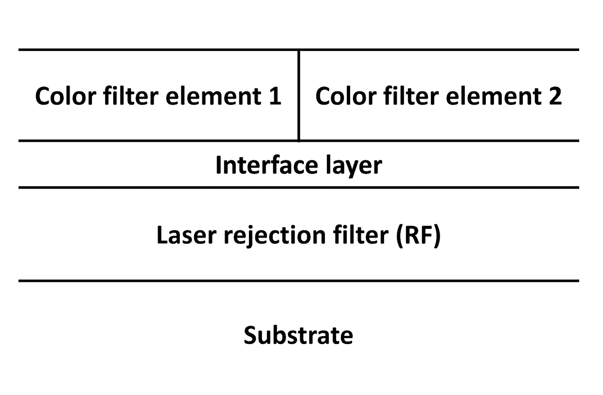
[0104]A schematic of an exemplary device comprising a laser-rejection filter and a color filtration layer comprising two three-cavity dielectric filter elements, is provided in FIG. 9. In order to fabricate an array of such devices, a laser rejection filter (RF) layer comprising a number of pairs of low index / high index layers is first deposited on the substrate. A layer of low refractive index material is next deposited. This layer acts as an interface between the laser rejection filter (RF) layer and the color filtration layer.
[0105]Table 1 shows the structure of the two three-cavity filter stacks of the device of FIG. 9, which act as color filter element 1 and color filter element 2, respectively. Color filter element 1 is designed to pass 600 nm light, while color filter element 2 is designed to pass 660 nm light. These multi-cavity filters comprise an alternating stack of reflectors and transparent cavities.
[0106]The reflectors in the multi-cavity filters of this color filtrati...
PUM
| Property | Measurement | Unit |
|---|---|---|
| Thickness | aaaaa | aaaaa |
| Thickness | aaaaa | aaaaa |
| Thickness | aaaaa | aaaaa |
Abstract
Description
Claims
Application Information
 - R&D Engineer
- R&D Manager
- IP Professional
- Industry Leading Data Capabilities
- Powerful AI technology
- Patent DNA Extraction
Browse by: Latest US Patents, China's latest patents, Technical Efficacy Thesaurus, Application Domain, Technology Topic.
© 2024 PatSnap. All rights reserved.Legal|Privacy policy|Modern Slavery Act Transparency Statement|Sitemap