Apparatus of Plural Charged-Particle Beams

a technology of charged particles and apparatuses, applied in the direction of electric discharge tubes, measurement devices, instruments, etc., can solve the problems of reducing the yield to a great degree, reducing the efficiency of conventional yield management tools with optical beams, and not providing throughputs competent for mass production, etc., to achieve high collection efficiency, low crosstalk level, and high inspection resolution

Active Publication Date: 2017-06-01
ASML NETHERLANDS BV
View PDF22 Cites 63 Cited by
  • Summary
  • Abstract
  • Description
  • Claims
  • Application Information

AI Technical Summary

Benefits of technology

[0017]The object of this invention is to provide a secondary projection imaging system of a multi-beam apparatus, which makes the secondary electron detection with both high collection efficiency and low cross-talk level even if the landing energies and / or currents of a plurality of beamlets change within large ranges. As a yield management tool in semiconductor manufacturing industry, the multi-beam apparatus therefore can achieve high inspection resolution and high inspection throughput in many application conditions.
[0027]In one embodiment, the zoom lens comprises a first zoom sub-lens and a second zoom sub-lens, and the second zoom sub-lens is between the first zoom sub-lens and the transfer plane. The anti-scanning deflection unit is between the first and second zoom sub-lenses. The anti-scanning deflection unit deflects the plurality of secondary electron beams incident to the second zoom sub-lens along the secondary optical axis. The secondary projection imaging system comprises a field lens placed at the transfer plane to reduce radial shifts and tilt angles of the plurality of secondary electron beams incident to the projection lens. The secondary projection imaging system comprises a secondary beam-limit aperture plate with one or more openings, and that one or one of the more openings is placed at a position of the second crossover to cut off peripheral electrons of the plurality of secondary electron beams. The secondary projection imaging system comprises a field lens placed at the transfer plane to bend the plurality of secondary electron beams to keep the position of the second crossover when observing the surface in different conditions.
[0043]In one embodiment, the zoom lens comprises a first zoom sub-lens and a second zoom sub-lens, and the second zoom sub-lens is between the first zoom sub-lens and the second field lens. The anti-scanning deflection unit respectively deflects the plurality of slow secondary electron beams in the SSE mode and the plurality of backscattered electron beams in the BSE mode incident to the second zoom sub-lens along the secondary optical axis. The secondary projection imaging system comprises a first secondary beam-limit aperture plate and a second secondary beam-limit aperture plate, each having one or more openings. In the SSE mode one opening of the first secondary beam-limit aperture plate is placed at the SSE crossover to cut off peripheral electrons of the plurality of slow secondary electron beams, and in the BSE mode one opening of the second secondary beam-limit aperture plate is placed at the BSE crossover to cut off peripheral electrons of the plurality of backscattered electron beams. The SSE crossover and the BSE crossover are set at a common position by adjusting the first field lens and the second field lens respectively. The secondary projection imaging system comprises a third secondary beam-limit aperture plate with one or more openings, and that one or one of the more openings is placed at the common position in each of the SSE mode and the BSE mode. The secondary projection imaging system comprises a stigmator placed close to the third secondary beam-limit aperture plate, which compensates astigmatism aberrations of the plurality of slow-secondary-electron spots and the plurality of backscattered-electron spots in the SSE mode and the BSE mode respectively due to the beam separator.
[0054]In one embodiment, the imaging system may further comprise a plate with at least one opening, one opening of the plate being as a beam-limit aperture for reducing sizes of the plurality of charged particle beams on the detection device. The plate includes a plurality of selectable openings with different sizes. The plate locates at a crossover of the plurality of charged particle beams between the projecting lens and the detection device.
[0055]In one embodiment, the imaging system may further comprise a stigmator for reducing astigmatism of the plurality of charged particle beams. The stigmator locates at a crossover of the plurality of charged particle beams.

Problems solved by technology

For manufacturing semiconductor IC chips, pattern defects and / or uninvited particles (residuals) inevitably appear on surfaces of wafers / mask during fabrication processes, which reduce the yield to a great degree.
Accordingly, the conventional yield management tools with optical beam gradually become incompetent due to diffraction effect, and yield management tools with electron beam are more and more employed.
Currently, the yield management tools with electron beam employ the principle of scanning electron microscope (SEM) with a single electron beam, which therefore can provide higher resolution but can not provide throughputs competent for mass production.
Although the higher and higher beam currents can be used to increase the throughputs, the superior spatial resolutions will be fundamentally deteriorated by Coulomb Effect which increases with the beam current.
Due to the emission of the secondary electrons conforms Lambert's law and has a large energy spread, all secondary electrons of each secondary electron beam can not be fully focused into the corresponding detection element.
Hence the plurality of detection elements can only provide high collection efficiency and low cross-talk level for some specific applications.

Method used


Image

  • Apparatus of Plural Charged-Particle Beams
  • Apparatus of Plural Charged-Particle Beams
  • Apparatus of Plural Charged-Particle Beams

Examples


Embodiment Construction

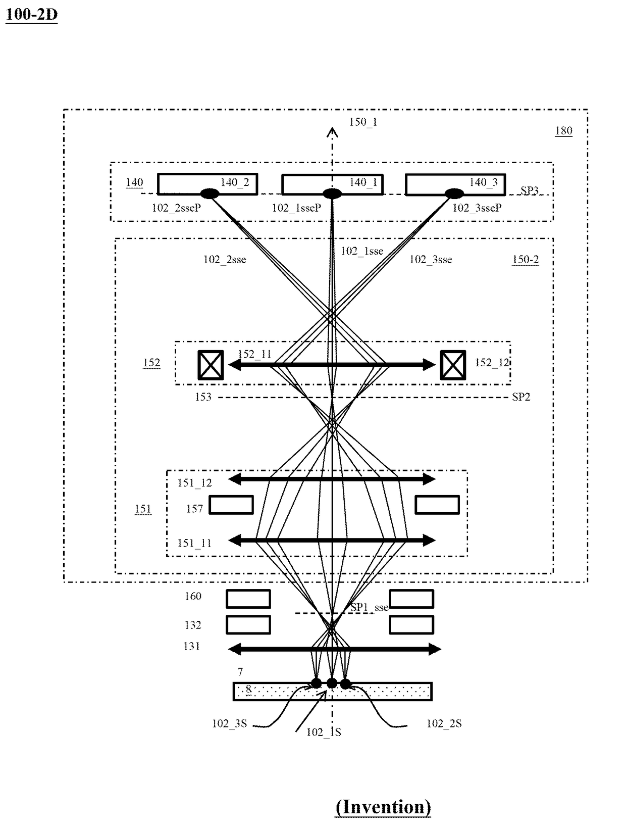
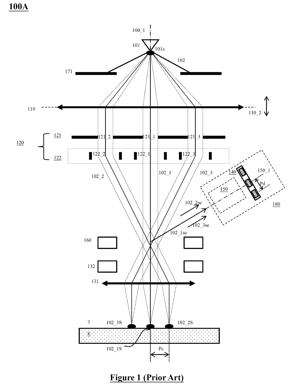
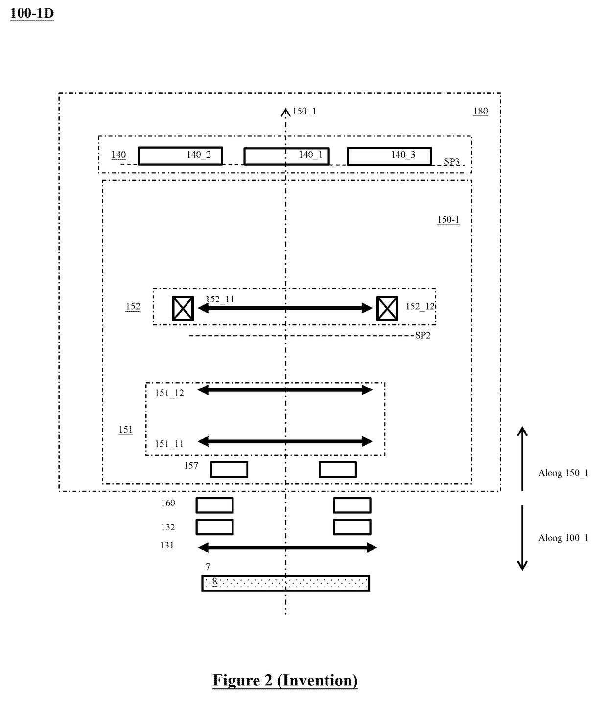
[0082]Various example embodiments of the present invention will now be described more fully with reference to the accompanying drawings in which some example embodiments of the invention are shown. Without limiting the scope of the protection of the present invention, all the description and drawings of the embodiments will exemplarily be referred to an electron beam. However, the embodiments are not used to limit the present invention to specific charged particles.

[0083]In the drawings, relative dimensions of each component and among every component may be exaggerated for clarity. Within the following description of the drawings the same or like reference numbers refer to the same or like components or entities, and only the differences with respect to the individual embodiments are described.

[0084]Accordingly, while example embodiments of the invention are capable of various modifications and alternative forms, embodiments thereof are shown by way of example in the drawings and wi...


PUM


Abstract

A secondary projection imaging system in a multi-beam apparatus is proposed, which makes the secondary electron detection with high collection efficiency and low cross-talk. The system employs one zoom lens, one projection lens and one anti-scanning deflection unit. The zoom lens and the projection lens respectively perform the zoom function and the anti-rotating function to remain the total imaging magnification and the total image rotation with respect to the landing energies and / or the currents of the plural primary beamlets. The anti-scanning deflection unit performs the anti-scanning function to eliminate the dynamic image displacement due to the deflection scanning of the plural primary beamlets.

Description

CLAIM OF PRIORITY[0001]This application claims the benefit of priority of U.S. provisional application No. 62 / 260,822 entitled to Ren et al. filed on Nov. 30, 2015 and entitled “Apparatus of Plural Charged-Particle Beams”, the entire disclosures of which are incorporated herein by reference.CROSS REFERENCE TO RELATED APPLICATIONS[0002]This application is related to U.S. application Ser. No. 15 / 065,342 entitled to Ren et al. filed on Mar. 9, 2016 and entitled “Apparatus of Plural Charged-Particle Beams”, the entire disclosures of which are incorporated herein by reference.[0003]This application is related to U.S. application Ser. No. 15 / 078,369 entitled to Ren et al. filed on Mar. 23, 2016 and entitled “Apparatus of Plural Charged-Particle Beams”, the entire disclosures of which are incorporated herein by reference.[0004]This application is related to U.S. application Ser. No. 15 / 150,858 entitled to Liu et al. filed on May 10, 2016 and entitled “Apparatus of Plural Charged-Particle B...

Claims


Application Information

Patent Timeline
Patent Type & Authority Applications(United States)
IPC IPC(8): H01J37/28H01J37/14H01J37/153H01J37/244H01J37/20
CPCH01J37/28H01J37/244H01J2237/1532H01J37/153H01J37/14H01J37/20H01J37/145H01J37/05G01N23/2251H01J37/141H01J37/292H01J2237/0453H01J2237/24465H01J2237/24592H01J2237/2806H01J2237/2817
Inventor REN, WEIMINGLIU, XUEDONGHU, XUERANGCHEN, ZHONGWEI
Owner ASML NETHERLANDS BV
Why Eureka
Try Eureka