

Methods of forming silicon germanium tin films and structures and devices including the films
a technology of silicon germanium tin and tin, applied in the direction of basic electric elements, electrical apparatus, semiconductor devices, etc., can solve the problems of high cost, poor high-volume manufacturing, and inability to meet the needs of high-volume manufacturing, and achieve the effect of low throughput times
- Summary
- Abstract
- Description
- Claims
- Application Information
AI Technical Summary
Benefits of technology
Problems solved by technology
Method used
Image

Examples
Embodiment Construction
[0024]The description of exemplary embodiments of methods, systems, structures, and devices provided below is merely exemplary and is intended for purposes of illustration only; the following description is not intended to limit the scope of the disclosure or the claims. Moreover, recitation of multiple embodiments having stated features is not intended to exclude other embodiments having additional features or other embodiments incorporating different combinations of the stated features.
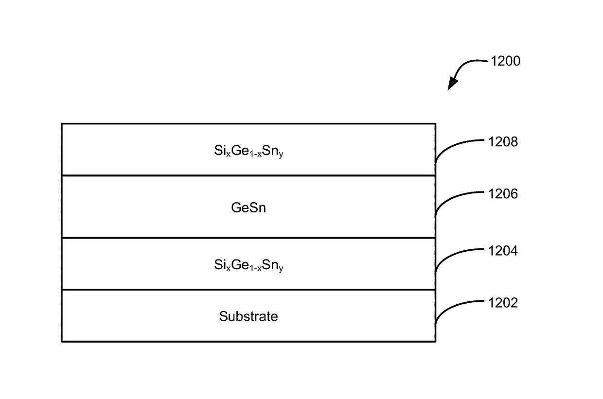
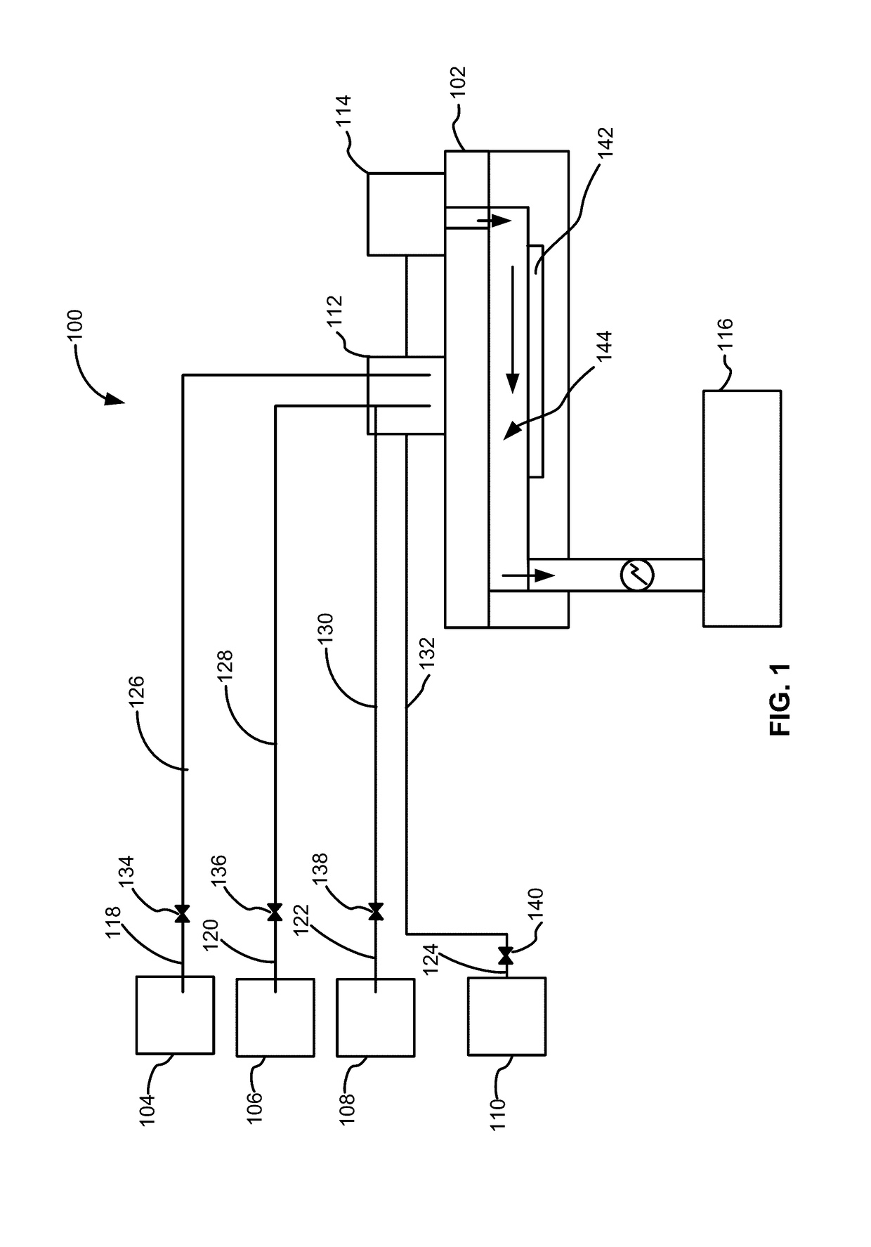
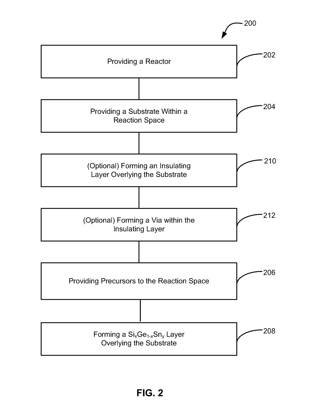
[0025]The present disclosure relates, generally, to methods of forming layers, such as crystalline alloy layers including silicon, germanium, and tin, overlying a substrate. The silicon germanium tin (SixGe1−xSny) layers can include additional elements, such as carbon, which forms part of a crystalline lattice with the silicon germanium tin layer and / or dopants (e.g., p-type dopants, such as boron (B) and / or n-type dopants, such as phosphorous (P) and Arsenic (As)).
[0026]Exemplary SixGe1−xSny layers...
PUM
 Abstract
Description
Claims
Application Information