Electrically and Magnetically Enhanced Ionized Physical Vapor Deposition Unbalanced Sputtering Source

a technology of ionized physical vapor and target material, which is applied in the direction of vacuum evaporation coating, semiconductor/solid-state device details, coatings, etc., can solve the problems of unbalanced magnetic field lines on the cathode target surface that form a magnetron configuration from the center, and achieve the effect of eliminating negative voltage bias

Inactive Publication Date: 2017-06-22
IONQUEST LLC
View PDF7 Cites 13 Cited by
  • Summary
  • Abstract
  • Description
  • Claims
  • Application Information

AI Technical Summary

Benefits of technology

[0006]The disclosed embodiments relate to an electrically and magnetically enhanced I-PVD unbalanced magnetron and non-magnetron apparatus and method for sputtering. Magnetic field geometry of the electrically and magnetically enhanced unbalanced magnetron sputtering source has an unbalanced magnetron configuration on a cathode target surface. Magnetic field lines that form a magnetron configuration on the cathode target surface are unbalanced from the center. In some embodiments, magnetic field lines are unbalanced from the edges. The unbalanced magnetic field lines are terminated on magnet assembly positioned inside an additional electrode that is electrically isolated from ground and positioned around the cathode target. The additional electrode is connected to a power supply that can generate a positive, negative or high frequency bipolar voltage with a frequency in the range of 100 KHz to 100 MHz. In some embodiments, the additional electrode is connected to the power supply that generates an RF voltage. In some embodiments, the additional electrode can be made from cathode target material. In some embodiments...

Problems solved by technology

Magnetic field lines that form a magnetron configuration on the cathode target surface are u...

Method used


Image

  • Electrically and Magnetically Enhanced Ionized Physical Vapor Deposition Unbalanced Sputtering Source
  • Electrically and Magnetically Enhanced Ionized Physical Vapor Deposition Unbalanced Sputtering Source
  • Electrically and Magnetically Enhanced Ionized Physical Vapor Deposition Unbalanced Sputtering Source

Examples


Embodiment Construction

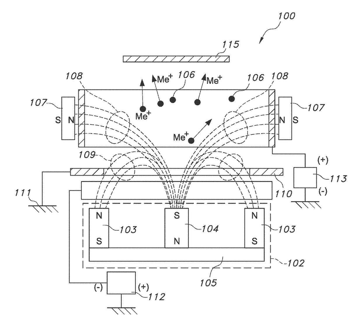
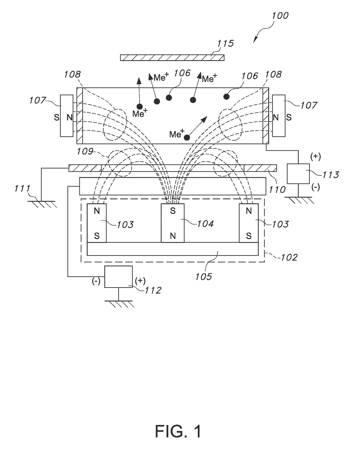
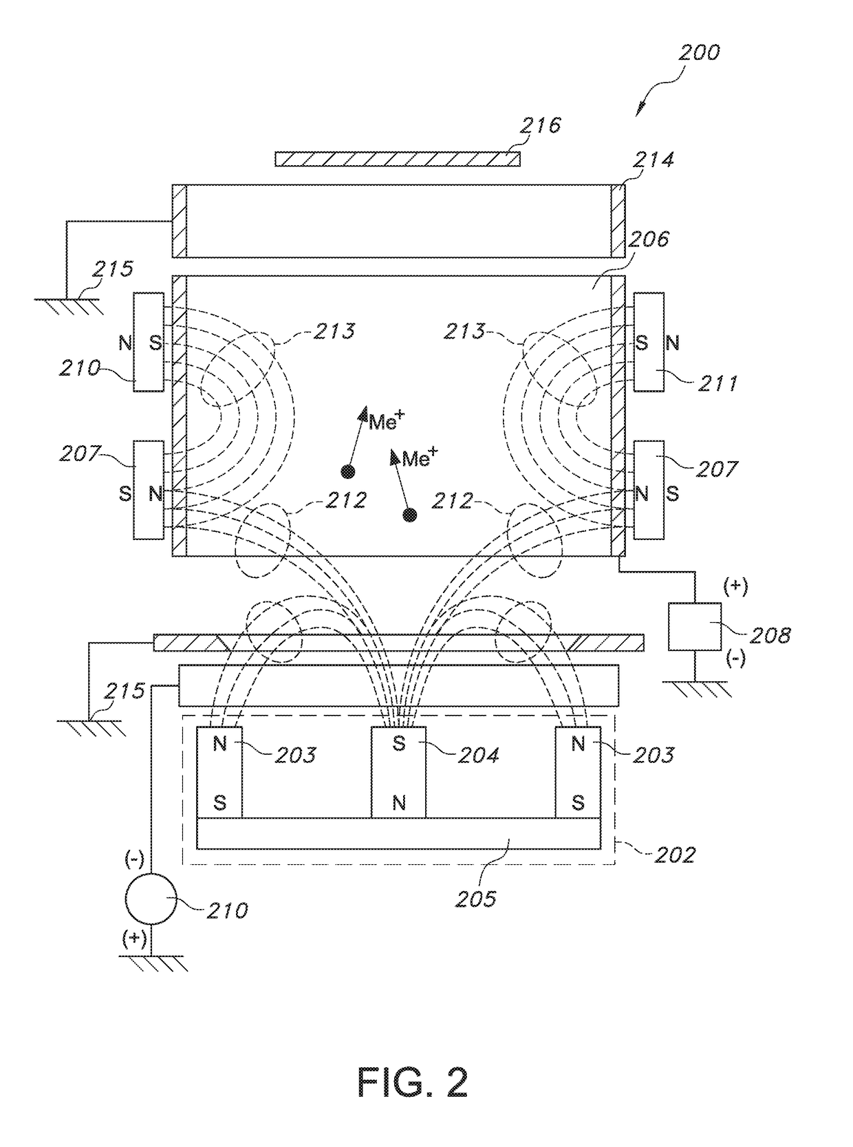
[0034]FIG. 1 shows a cross-sectional view 100 of magnetic field lines in an embodiment in which an additional electrode 106 has one magnet assembly. A cathode magnet assembly 102 includes magnets 103, 104 and magnetic pole piece 105. The cathode magnet assembly 102 forms a magnetron configuration with magnetic field lines 109 near a target surface 101. A portion of the magnetic field lines 108 cross the additional electrode 106 and terminate on the magnet 107. The additional electrode 106 is connected to a power supply 113. The power supply 113 can generate positive voltage. In an embodiment, the power supply 113 can generate high frequency bipolar asymmetrical voltages. In an embodiment, the power supply 113 can generate a radio frequency (RF) voltage with frequencies in the range of 100 KHz to 100 MHz. In an embodiment, the power supply 113 can generate a negative voltage. When the power supply 112 generates power and a magnetron discharge is formed near the cathode target 101, el...


PUM

PropertyMeasurementUnit
Poweraaaaaaaaaa
Poweraaaaaaaaaa
Poweraaaaaaaaaa

Abstract

An electrically and magnetically enhanced ionized physical vapor deposition (I-PVD) magnetron apparatus and method is provided for sputtering material from a cathode target on a substrate, and in particular, for sputtering ceramic and diamond-like coatings. The electrically and magnetically enhanced magnetron sputtering source has unbalanced magnetic fields that couple the cathode target and additional electrode together. The additional electrode is electrically isolated from ground and connected to a power supply that can generate positive, negative, or bipolar high frequency voltages, and is preferably a radio frequency (RF) power supply. RF discharge near the additional electrode increases plasma density and a degree of ionization of sputtered material atoms.

Description

CROSS-REFERENCE TO RELATED APPLICATIONS[0001]This application claims the benefit of U.S. Provisional Application Ser. No. 62 / 270,356, filed Dec. 21, 2015, the disclosure of which is incorporated herein by reference in its entirety. U.S. application Ser. No. ______ entitled “Capacitive Coupled Plasma Source for Sputtering and Resputtering”, U.S. application Ser. No. ______ entitled “Magnetically Enhanced High Density Plasma-Chemical Vapor Deposition Plasma Source for Depositing Diamond and Diamond-Like Films”, and U.S. application Ser. No. ______ entitled “Magnetically Enhanced Low Temperature-High Density Plasma-Chemical Vapor Deposition Plasma Source for Depositing Diamond and Diamond Like Films” filed concurrently herewith are incorporated herein by reference in their entireties.BACKGROUND[0002]Field[0003]The disclosed embodiments generally relate to an ionized physical vapor deposition (I-PVD) apparatus and method for sputtering target material on a surface of a substrate. In par...

Claims


Application Information

Patent Timeline
IPC IPC(8): H01J37/34H01J37/32C23C14/35
CPCH01J37/3452C23C14/35H01J37/3417H01J37/321H01J37/32825H01J37/3464H01J37/3455H01J37/3435H01J37/3405C23C14/3485C23C14/345C23C14/354H01J37/345H01J37/3467C23C14/0605C23C14/14H01J37/3426C23C16/505H01L21/2855H01L21/76843H01L21/76871H01L21/76879H01L21/76882H01L23/5226H01L23/53238C23C14/0057
Inventor ABRAHAM, BASSAM HANNACHISTYAKOV, ROMAN
Owner IONQUEST LLC
Why Eureka
Try Eureka