Biosensor device
a biosensor and sensor technology, applied in the field of sensors, can solve the problems of affecting the yield factor of the prior sensor device b>1/b>, difficult control, and affecting the sensitivity of the sensor device, so as to improve the sensitivity, enhance the sensing signal strength, and remove the effect of environmental noise interferen
- Summary
- Abstract
- Description
- Claims
- Application Information
AI Technical Summary
Benefits of technology
Problems solved by technology
Method used
Image
Examples
first embodiment
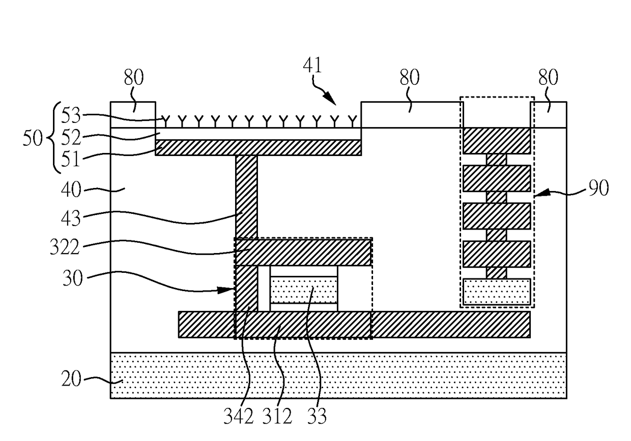
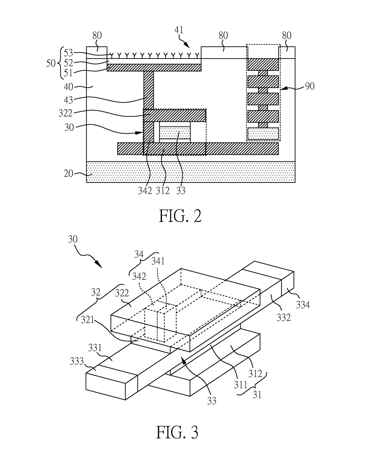
[0021]FIG. 2 shows the first embodiment of the biosensor device 2 according to the present invention. The biosensor device 2 includes a substrate 20, a sensing transistor 30, an isolation layer 40, and a main interface layer 50.
[0022]The substrate 20 can be made of semiconductor materials such as Si, Ge, SiC, GaAs, GaP, InP, InAs, InSb, SiGe, GaAsP, AlInAs, AlGaAs, GaInAs, GaInP, GaInAsP, or the combinations thereof.
[0023]The sensing transistor 30 is formed on the substrate 20.
[0024]To further describe the details of the semiconductor layer 33, FIG. 3 shows a perspective view of the sensing transistor 30 in the first embodiment of the present invention.
[0025]The sensing transistor 30 includes a bottom gate structure 31 with a bottom dielectric layer 311 and a bottom conductive layer 312, a top gate structure 32 with a top dielectric layer 321 and a top conductive layer 322, and a semiconductor layer 33. The bottom conductive layer 312 of the bottom gate structure 31 is electrically ...
second embodiment
[0046]FIG. 4 shows the second embodiment of the biosensor device 2 according to the present invention. The second embodiment is provided on the basic of the first embodiment. However, in the second embodiment, the bottom conductive layer 312 is electrically connected to the top conductive layer 322 through not only the first via hole 34, but also a second via hole 35. The second via hole 35 is coated with a dielectric material 351 and then filled with a conductive material 352. Accordingly, the bottom gate structure 31, the top gate structure 32, the first via hole 34 and the second via hole 35 vertically surround the semiconductor layer 33, and constitute a surrounding gate structure of the sensing transistor 30.
[0047]FIG. 5 shows a perspective view of the sensing transistor 30 in the second embodiment of the present invention. The structure of the semiconductor layer 33 in FIG. 5 is similar to that in FIG. 3, except that the existence of the second via hole 35. In this case, the b...
third embodiment
[0050]FIG. 6 shows the third embodiment of the biosensor device 2 according to the present invention. The third embodiment is provided on the basic of the second embodiment. However, in the third embodiment, the main interface conductive layer 51 is electrically connected to the top conductive layer 322 through not only the third via hole 43, but also a fourth via hole 44. Thus, the resistance of the connection between the first conductive layer 51 and the top conductive layer 322 can be reduced, and the strength of the gate signal can be maintained.
PUM
 Abstract
Description
Claims
Application Information
 - R&D
- Intellectual Property
- Life Sciences
- Materials
- Tech Scout
- Unparalleled Data Quality
- Higher Quality Content
- 60% Fewer Hallucinations
Browse by: Latest US Patents, China's latest patents, Technical Efficacy Thesaurus, Application Domain, Technology Topic, Popular Technical Reports.
© 2025 PatSnap. All rights reserved.Legal|Privacy policy|Modern Slavery Act Transparency Statement|Sitemap|About US| Contact US: help@patsnap.com


