Eureka AIR delivers breakthrough ideas for toughest innovation challenges, trusted by R&D personnel around the world.

Display device

a display device and display angle technology, applied in non-linear optics, instruments, optics, etc., can solve the problems of color shift phenomenon, increase the number of scan lines, and different colors seen from a side viewing angle, so as to reduce insufficient color saturation, the process yield rate or the aperture ratio of the display device can be improved, and the effect of reducing the problem of color shi

Active Publication Date: 2017-06-29
INNOLUX CORP
View PDF0 Cites 8 Cited by
  • Summary
  • Abstract
  • Description
  • Claims
  • Application Information

AI Technical Summary

Benefits of technology

The patent describes a display device that solves issues with current wide viewing angle technology such as low process yield rate and low aperture ratio. The device has a pixel electrode and a common electrode layer, with a difference in distance between them for the first and second pixel electrodes. This design allows for different brightness levels for the two electrodes, without compromising color accuracy. As a result, the process yield rate and aperture ratio of the display device are improved.

Problems solved by technology

However, when viewing a vertical alignment liquid crystal display device, due to the birefringence properties of liquid crystal molecules, there exists a phenomenon where colors seen from a side viewing angle are different from those seen from a direct viewing angle; namely, a phenomenon of color shift occurs.
However, such design increases a number of the thin film transistors and meanwhile increases a number of the scan lines.
It not only increases a probability of lowering the process yield rate, but also lowers the aperture rate of the liquid crystal display device.

Method used


Image

  • Display device
  • Display device
  • Display device

Examples


Embodiment Construction

[0035]Reference will now be made in detail to the exemplary embodiments of the disclosure, examples of which are illustrated in the accompanying drawings. Wherever possible, the same reference numbers are used in the drawings and the description to refer to the same or like parts.

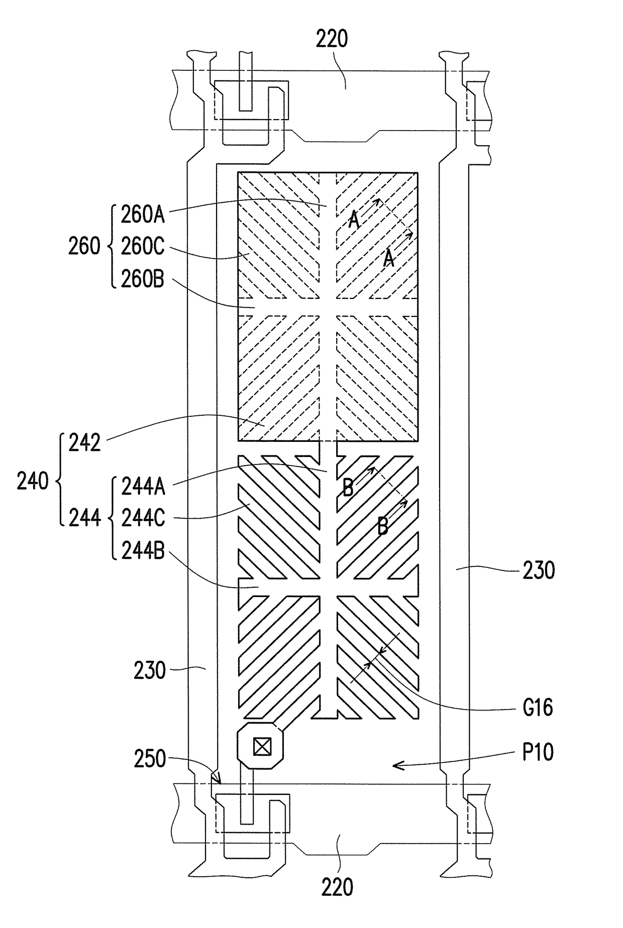
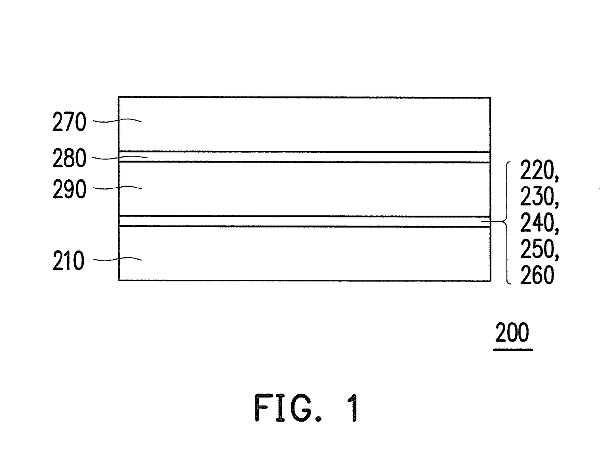
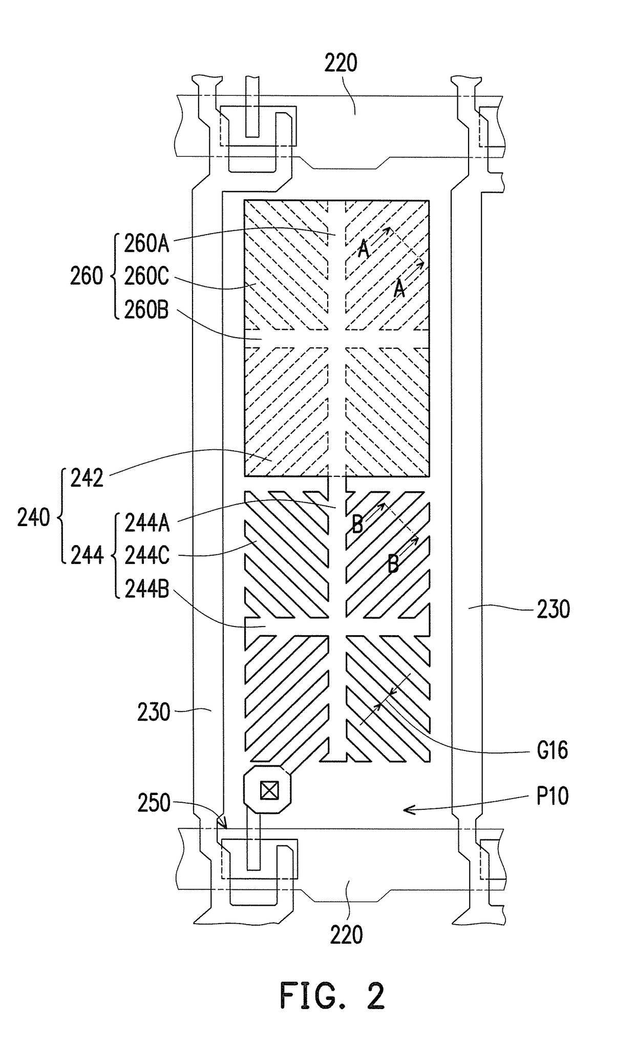
[0036]FIG. 1 is a cross-sectional simplified schematic view of a display device according to one embodiment of the disclosure. FIG. 2 is a top view of a single sub-pixel area of the display device of FIG. 1. Referring to FIGS. 1 and 2, a display device 200 according to one embodiment of the disclosure includes a first substrate 210, at least two scan lines 220, at least two data lines 230, at least a pixel electrode 240, at least an active component 250, a first interlayer 260, a second substrate 270, a common electrode layer 280, and a display medium layer 290. FIG. 2 only illustrates one single sub-pixel area. Upon referring to FIG. 2, an arrangement of at least two or more scan lines 220, at least two or...


PUM


Abstract

The disclosure provides a display device. The pixel electrode of the display device includes a first pixel electrode and a second pixel electrode having the same electric potential. The first interlayer is formed between the first substrate and the first pixel electrode. Adjacent two of the first strip-shaped branches of the first interlayer form a first gap to expose part of the first substrate. The common electrode layer is disposed over the second substrate. The pixel electrode is positioned between the first substrate and the display medium layer. The first pixel electrode extends to cover the first gap. A difference between a maximum distance between the first pixel electrode and the common electrode layer and a maximum distance between the second pixel electrode and the common electrode layer is 0.1 μm to 0.4 μm.

Description

CROSS-REFERENCE TO RELATED APPLICATION[0001]This application claims the priority benefit of China application serial no. 201511006036.1, filed on Dec. 29, 2015. The entirety of the above-mentioned patent application is hereby incorporated by reference herein and made a part of this specification.BACKGROUND OF THE INVENTION[0002]Field of the Invention[0003]The invention relates to a display device.[0004]Description of Related Art[0005]Nowadays, the market demands the liquid crystal display device to develop its functions towards high contrast ratio, no gray scale inversion, low color shift, high luminance, full color, high color saturation, high response speed, and a wide viewing angle. Currently, the technologies capable of meeting the requirement of a wide viewing angle include the twist nematic (TN) liquid crystal having a wide viewing film, the in-plane switching (IPS) liquid crystal display device, the fringe field switching liquid crystal display device, and the multi-domain ve...

Claims


Application Information

Patent Timeline
IPC IPC(8): G02F1/1343G02F1/1362
CPCG02F1/134309G02F1/136286G02F1/13439G02F1/137G02F2201/121G02F2201/123G02F2001/134345G02F2201/40G02F1/133345G02F1/133371G02F1/133707G02F1/1343G02F1/134345
Inventor HO, YU-SHENGLI, HSUEH-WENLIN, MAO-SHIANGCHEN, YING-JEN
Owner INNOLUX CORP
Why Eureka
Eureka Blog
Learn More