
Conductive composition and applications thereof

a technology of conductive composition and composition, applied in the field of flat lamps, can solve the problems of difficult separation easy breakage of glass substrate and supporter, uneven thickness ranging from 200 m to 250 m, etc., to reduce manufacturing costs, simplify manufacturing process, and low yield rate

Active Publication Date: 2009-10-20
AU OPTRONICS CORP
View PDF4 Cites 0 Cited by
  • Summary
  • Abstract
  • Description
  • Claims
  • Application Information

AI Technical Summary

Benefits of technology

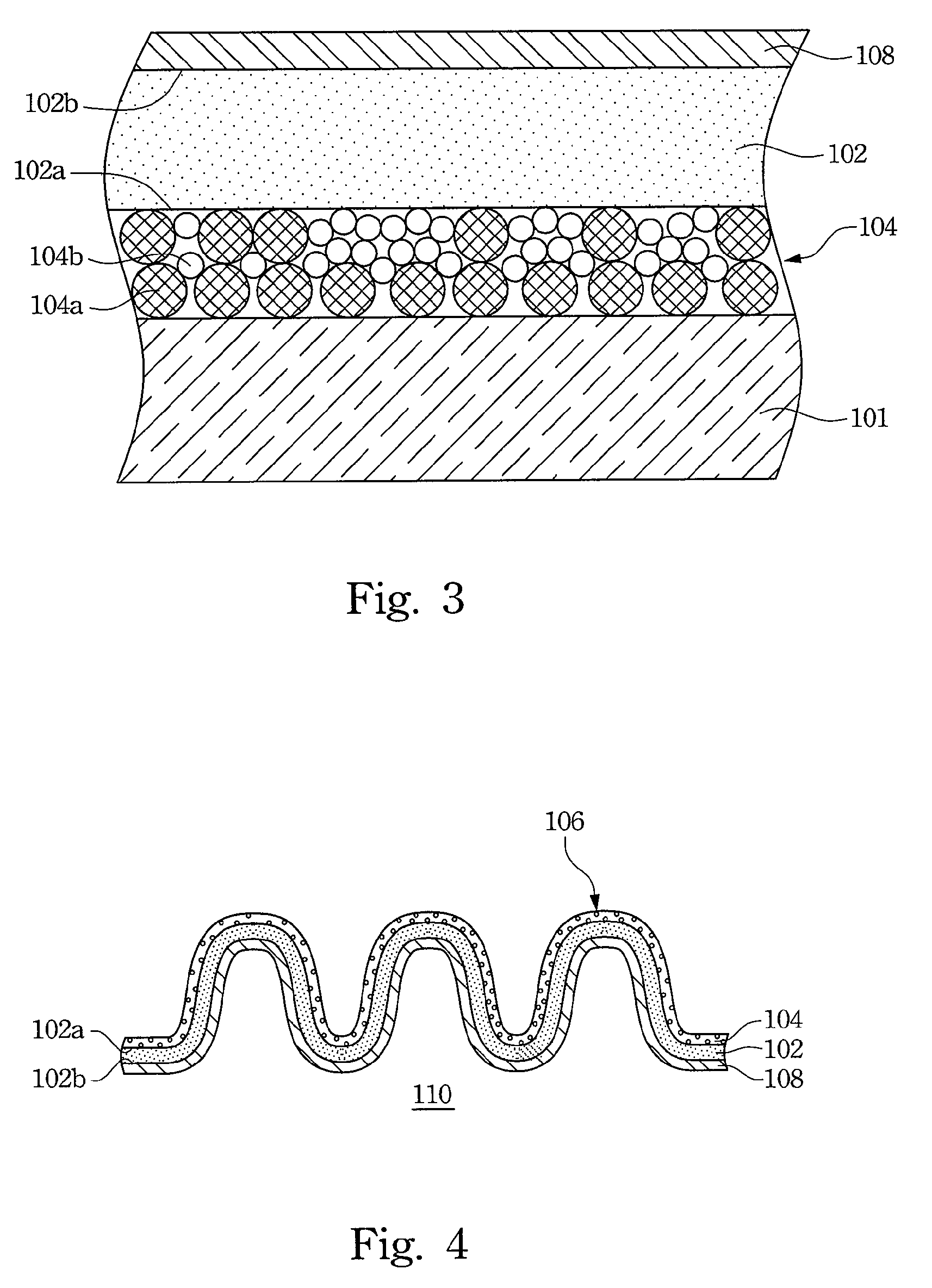
"The present invention provides a conductive composition for a flat lamp that avoids the problem of easily broken glass substrate. The composition includes metal powder, glass powder, and organic solvent. The amount of metal powder and glass powder suspended in organic solvent is larger than 60% of the solution. The diameter of metal powder ranges from 1 μm to 3 μm, and the diameter of glass powder ranges from 0.5 μm to 1 μm. The weight percentage of metal powder in the mixture is from 60% to 80%. The flat lamp comprises two substrates, gas, and a thin film electrode. The thin film electrode is on two end of the substrate and has a better thickness range from 5 μm-200 μm. The manufacturing method involves cleaning the substrate, printing a conductive coating layer, baking the substrate, and shaping the substrate and thin film electrode into a corrugated structure. The flat lamp can be completed by packaging two preliminary completed substrates together with the two fluorescence layers facing each other and a discharging space formed between the two substrates. The invention solves the conventional broken glass problem, simplifies the manufacturing process, lowers manufacturing cost, and increases product quality and yield rate."

Problems solved by technology

Once if the electrode layer and the supporter are attached together, it is very difficult to separate the glass substrate and the supporter after the glass substrate, electrode layer and fluorescence layer are cooled down.
The glass substrate and the supporter are easily broken when trying to separate them.
However, the drawbacks of this obtained electrode layer include the thicker thickness and uneven thickness ranging from 200 μm to 250 μm.
This not only increases production cost but also decreases product quality.

Method used


Image

  • Conductive composition and applications thereof
  • Conductive composition and applications thereof
  • Conductive composition and applications thereof

Examples


Embodiment Construction

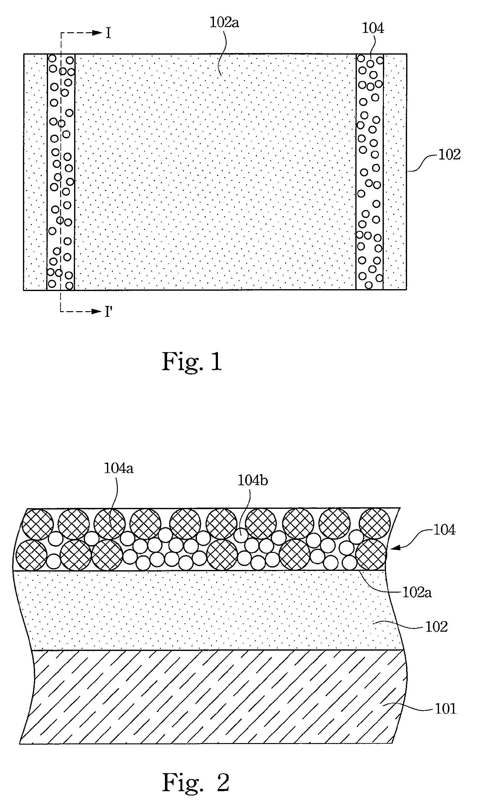
[0021]Please refer to FIG. 1, FIG. 1 is a schematic view of a glass substrate with electrode according to an embodiment of the invention. A glass substrate 102 is cleaned and placed on a supporter (not shown in FIG. 1). A printing process is performed on the substrate to form a conductive coating layer on the first surface 102a of the substrate 102. Bake the substrate 102 and sinter the conductive coating layer to form a thin film electrode 104 on the substrate 102. The thickness of the thin film electrode 104 ranges from 5 μm-200 μm, but the preferred thickness of the thin film electrode 104 ranges from 10 μm-50 μm and the more preferred thickness ranges from 10 μm-30 μm.

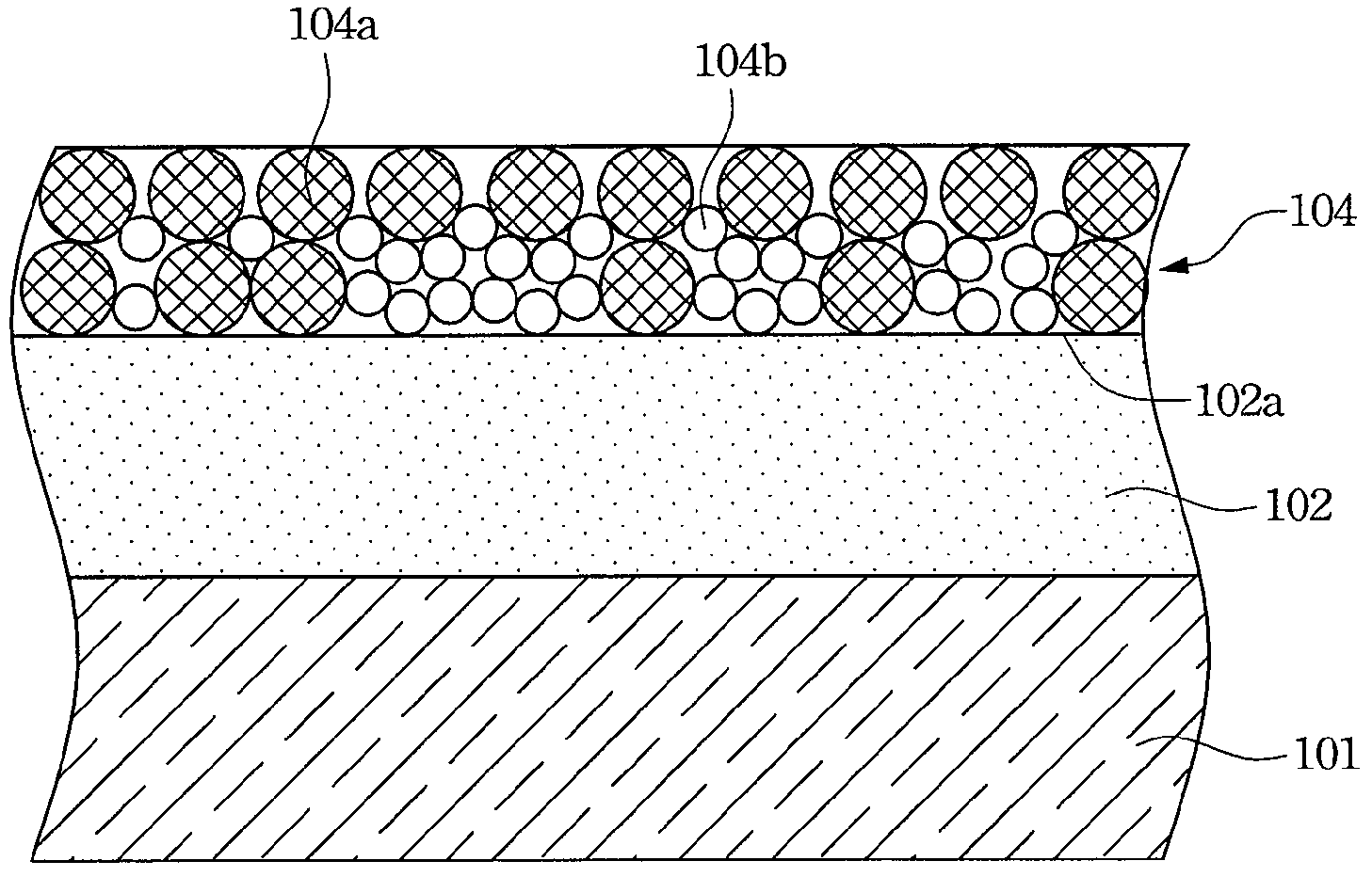
[0022]Please also refer to FIG. 2, FIG. 2 is a cross sectional views along I-I′ shown in FIG. 1. The substrate 102 is preferably placed on the supporter 101. The thin film electrode 104 is preferably formed on the first surface 102a of the substrate 102.

[0023]The thin film electrode 104 is made of a conductive comp...


PUM

PropertyMeasurementUnit
thicknessaaaaaaaaaa
thicknessaaaaaaaaaa
thicknessaaaaaaaaaa

Abstract

A conductive composition and applications thereof are provided. The conductive composition comprises metal powder and glass powder. The diameter of metal powder ranges from 1 μm to 3 μm. The diameter of glass powder ranges from 0.5 μm to 1 μm. Weight percentage of the metal powder is from 60% to 98%. The conductive composition could be applied to manufacture the electrodes of a flat lamp.

Description

RELATED APPLICATIONS[0001]The present application is based on, and claims priority from, Taiwan Patent Application Serial Number 95129253, filed Aug. 9, 2006, the disclosure of which is hereby incorporated by reference herein in its entirety.BACKGROUND[0002]1. Field of Invention[0003]The present invention relates to a flat lamp. More particularly, the present invention relates to a conductive composition used in a plat lamp.[0004]2. Description of Related Art[0005]Flat lamp featured by its luminescence efficiency, uniformity and large-area luminescence is usually applied to backlight module of liquid crystal display or other devices. Flat lamp comprises an upper substrate and a lower substrate which form a panel-like structure. Each of the outer surfaces of the upper substrate and the lower substrate contains an electrode layer. Each of the inner surfaces of the two substrates contains a fluorescence layer. The upper substrate and the inner substrate are attached together with a spa...

Claims


Application Information

Patent Timeline
Patent Type & Authority Patents(United States)
IPC IPC(8): H01J1/62
CPCH01B1/16H01B1/22H01J9/02H05B33/28H01J61/0675H01J61/305H01J65/046H01J9/248
Inventor LIN, YU-KAI
Owner AU OPTRONICS CORP
Learn More